Semiconductor / TFT / Diode Measurements
This section describes in detail all measurement modules in the Semiconductor / TFT / Diode family of the Mikrofab measurement and analysis software. For each module it covers the purpose, the measured quantities, complete parameter tables, the formulas for the computed metrics, the types of plots produced, the simulation (mock) behavior, and the output files. In the application the modules are listed in the Measurement workspace, in the left navigation tree under three categories: Transistor, Diode, Resistivity, and Reliability / Thermal-Map.
This section explains the ways to measure how a semiconductor device (transistor, diode, thin film) "behaves" electrically. We apply controlled voltage/current to the device, read its response (its current), and from this extract the device's character. Just as a doctor runs different tests on a patient and reaches a diagnosis by looking at a single chart, each measurement mode illuminates a different aspect of the device.
Physical background: Each measurement is, in fact, an indirect window into the device's band structure, carrier density, and traps: the voltage we apply changes the electric field and the energy barriers inside the device, and the current we read is the carriers' response to this new state. That is why different sweep schemes (DC, pulsed, temperature-swept) reveal different physical quantities from the same device; a single measurement is incomplete on its own, while the ensemble of modules gives the "complete picture" of the device.
- Why it is done: To understand whether the device we make/purchase works, how good it is, and why it degrades.
- What it teaches / measures: The fundamental numbers that describe the device, such as threshold voltage, mobility, on/off ratio, rectification, and resistance.
- Where it is used: Research laboratories, quality control, production lines, and failure analysis.
Common Concepts and Shared Parameters
All measurement modules share a common infrastructure (app/measurement/sweep_engine.py, runner.py, base.py). This infrastructure gives every module the following behaviors:
- Sweep engine and dispatch:
SweepEnginecalls the relevant runner class according to the selected mode;MeasurementRunnersaves the result and returns(points, summary, file_paths). - Crash-safe intermediate save: While the measurement is running, each measurement point is first written to a temporary
*_partial.csvfile. If the measurement completes successfully this temporary file is deleted; if an error or crash occurs it is left on disk (no data loss). - Safe shutdown: At the end of every measurement — success, error, or cancellation — the SMU outputs are turned off (
output_all_off) and relays are opened where required. On error/cancellation the biases are brought to a safe value (0 V / output OFF). - Compliance (current/voltage limit) protection: If the device reaches compliance at a measurement point, the measurement is stopped for safety and a warning is produced indicating at which point (out of how many) it stopped.
- Sweep direction (hysteresis):
Forward(forward only),Reverse(reverse only), orDual(forward + reverse; hysteresis). In Dual the forward and reverse directions are labeled as separate segments; hysteresis metrics are computed only in Dual. - Hardware error queue: After SCPI/TSP operations the device's error queue is read safely; errors are not swallowed but surfaced in a meaningful way.

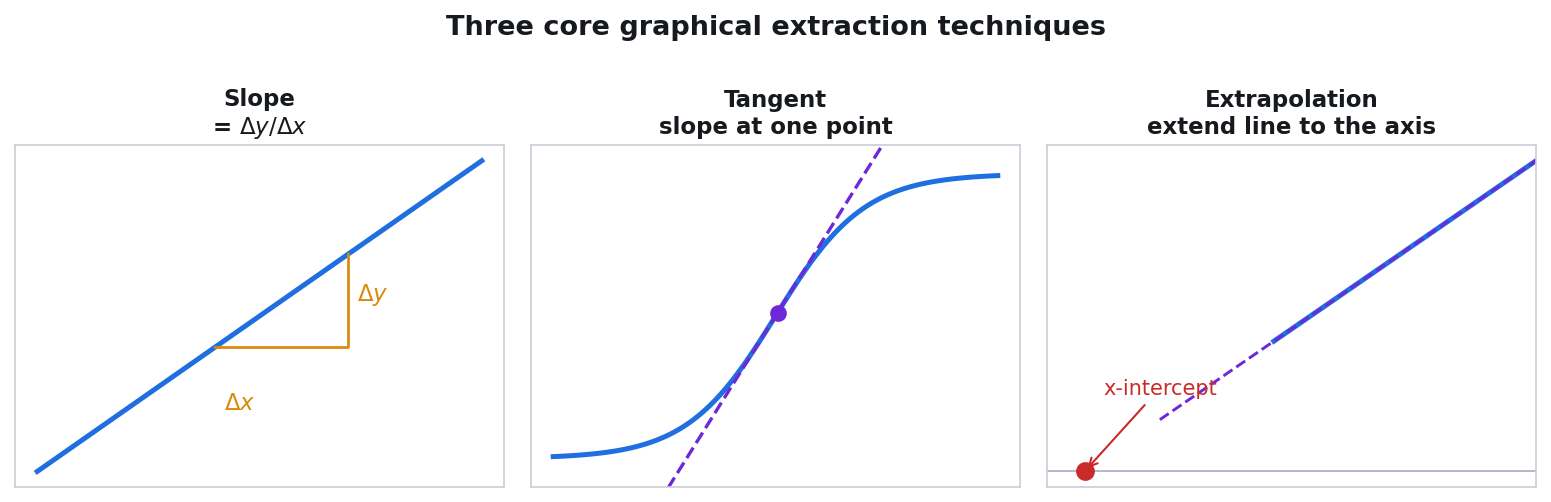
Almost all parameters in this section are read from the measurement plot with three fundamental operations: the slope of a line (Δy/Δx), the tangent at a point (the instantaneous slope there), and extrapolation that carries the line onto an axis. In most cases a suitable transformation (e.g., log I_d, √I_d, ln I, 1/C², log–log) is applied first so that the region of interest turns into a straight line.
- Step: the physical region of interest is selected (linear, saturation, sub-threshold, exponential arm …) and the axis is transformed if needed.
- Step: a line/tangent is fitted to this region and the slope is taken as Δy/Δx.
- Result: if needed, the line is carried onto an axis by extrapolation and the intercept is read; the slope and intercept are converted to the parameter via the relevant formula.
Common SMU parameters (in all modules)
The following basic parameters (BaseSweepParameters) are present in nearly every module and can take their default values from a single place via Settings → Central Defaults.
| Parameter | Unit | Description | Default |
|---|---|---|---|
drain_current_compliance | A | Drain current limit | 1e-4 |
gate_current_compliance | A | Gate current limit | 1e-6 |
voltage_limit | V | Voltage limit (voltage compliance in current-source mode) | 20.0 |
power_limit | W | Power limit | 2.0 |
nplc | — | Integration time (Number of Power Line Cycles); high = low noise, slow | 1.0 |
settling_time_s | s | Settling wait after a step/stage change | 0.05 |
measurement_delay_s | s | Pre-measurement wait for each point | 0.02 |
averages | — | Number of readings averaged per point | 1 |
sweep_direction | — | Forward / Reverse / Dual | Forward |
log_scale | — | Show the live plot logarithmically | False |
enable_autorange | — | Enable the device autorange preference | True |
voltage_limit and compliance values are validated against the safety limits (max_abs_voltage, max_current_compliance) at the start of every measurement; if a limit is exceeded the measurement does not start at all.Geometry parameters (for mobility/threshold)
In TFT/FET modules the computation of mobility (µFE / µ_sat) and the saturation threshold requires optional geometry inputs. If they are not entered, the corresponding metric is skipped (0 = not entered).
| Parameter | Unit | Description | Default |
|---|---|---|---|
w_um | µm | Channel width (W) | 0.0 |
l_um | µm | Channel length (L) | 0.0 |
cox_nf_cm2 | nF/cm² | Gate insulator capacitance (Cox) | 0.0 |
Unit conversions are automatic in the formulas: Cox_F = cox_nf_cm2 × 1e-9 (F/cm²), W/L is dimensionless; the result comes out directly in cm²/Vs.
Output files (all modules)
When each measurement is saved, a raw-data CSV (each row a MeasurementPoint: timestamp, mode, Vds/Vgs set+measured, Ids, Igs, compliance, elapsed time) and a summary (computed metrics) are produced. The file base name is derived from the context (e.g., TFT1_TRANSFER_YYYYMMDD_HHMMSS), with an optional prefix/suffix (e.g., IGZO_TFT1_TRANSFER_..._fresh). The summary is also optionally saved to the measurement database.
A. Transistor / FET / TFT Modules
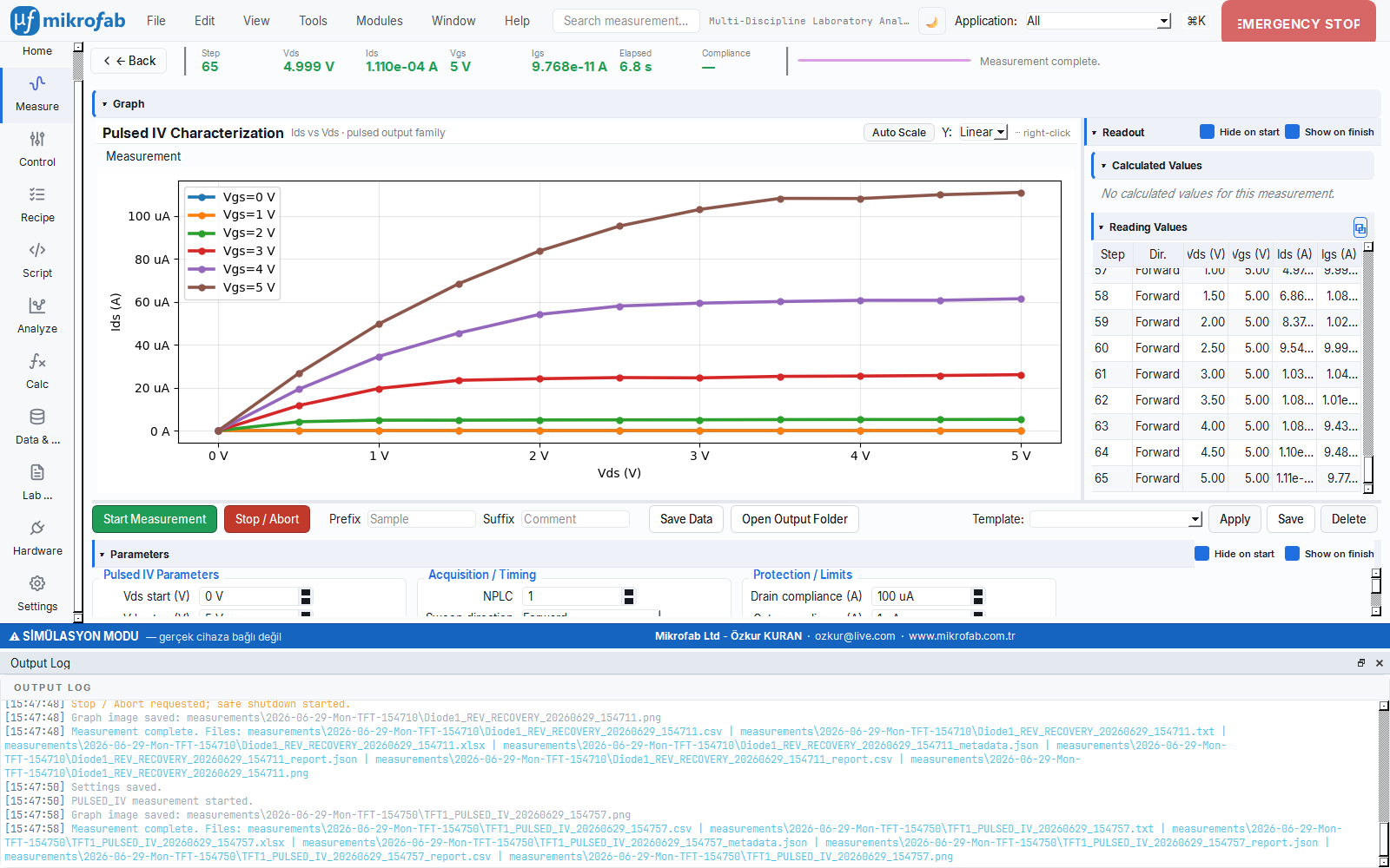
A.1 Output Characteristic — Vds–Vgs (Output / Id–Vd)
Think of a transistor as a faucet: the gate voltage (V_GS) sets how far the faucet is open, while the drain voltage (V_DS) sets the pressure in the pipe. This measurement holds the faucet at different fixed openings and, while slowly increasing the pressure (V_DS), monitors the flowing current (I_DS). The resulting family of curves summarizes how much power the transistor can carry as a switch or amplifier and how much gain it can provide. For each faucet opening a separate "pressure-flow" curve emerges; the higher and smoother the curves, the stronger the device.
Physical background: At low V_DS the channel behaves like a conductive resistor from end to end, so I_DS increases approximately linearly with V_DS (linear/triode region). When V_DS exceeds V_GS−V_th, the channel "pinches off" at the drain end (pinch-off): the extra voltage now drops across the depleted region instead of increasing the current, and the curve flattens (saturation region). The slight upward slope in saturation is channel-length modulation (λ); curves at higher V_GS sit higher because there are more carriers in the channel. The sharp onset + flat plateau you see "at a glance" is the signature of a healthy transistor.
- Why it is done: To see how much current the transistor can carry as a switch/amplifier, at which V_DS it enters saturation, and its power/gain limits.
- What it teaches / measures: R_on = on-state resistance in the linear region (low = little conduction loss); r_o = output resistance in saturation (high = close to an ideal current source, high gain); λ = channel-length modulation, the deviation of the saturation slope from zero (small = flatter/more ideal); knee = the knee voltage where it transitions from linear to saturation; g_m = transconductance (how effectively the gate drives the current); A_v = g_m·r_o = intrinsic voltage gain.
- Typical values and their interpretation: the knee is usually on the order of V_GS−V_th; in a good device r_o ≫ R_on (ratio of hundreds–thousands) and the saturation plateau is well defined; A_v in the tens–hundreds is good analog gain; the smaller λ is (≪1 1/V), the more ideal the output.
- Common mistakes / cautions: keeping the V_DS range too short so saturation is never reached (r_o and λ cannot be extracted); hitting compliance and clipping the top of the curve (the saturation current is read incorrectly); forgetting that the knee voltage must be found from the peak of the second derivative (|d²I/dV²|) rather than by eye.
- Where it is used: device selection/validation in power-switch and analog-circuit design; process validation and quality control.
Module: measure.iv · Navigation: Output — Vds–Vgs
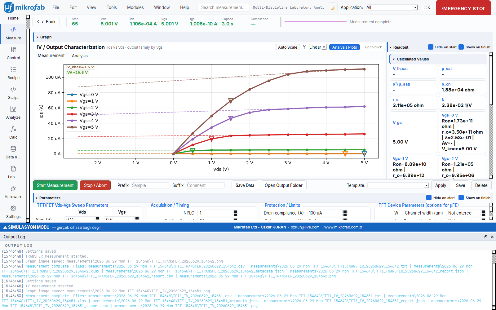
Purpose: For each fixed V_GS step, it sweeps the drain voltage (V_DS) to measure the transistor's output curve family. It reveals the linear and saturation regions.
What it measures: At each (V_GS, V_DS) point, the drain current I_DS and the gate leakage I_GS. V_GS is a parameter (the gate step), V_DS is the swept axis. In Dual mode hysteresis is applied only on the swept V_DS axis; V_GS is stepped in a single direction.
| Parameter | Unit | Description | Default |
|---|---|---|---|
vds_start / vds_stop / vds_step | V | Drain sweep start/stop/step | 0.0 / 5.0 / 0.5 |
vgs_start / vgs_stop / vgs_step | V | Gate step start/stop/step | 0.0 / 5.0 / 1.0 |
w_um / l_um / cox_nf_cm2 | µm / µm / nF/cm² | Geometry (for µ_sat/Vth_sat, opt.) | 0.0 |
| Common SMU parameters | — | NPLC, compliance, settling, averages, etc. | (table above) |
Computed metrics (iv_analysis.py; for each V_GS curve + headline values):
| Metric | Formula / Method | Unit |
|---|---|---|
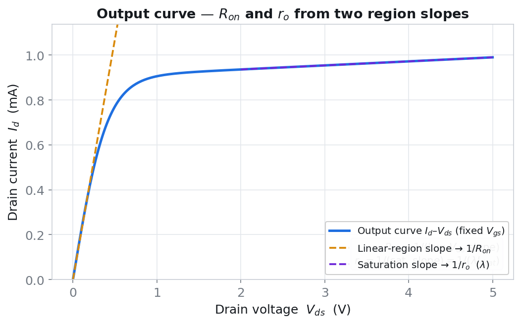
| R_on (on resistance) | Inverse of the I_DS–V_DS fit slope in the low-V_DS linear region (|V| ≤ min(0.5, 0.05·V_max)): R_on = |1/slope| | Ω |
| r_o (output resistance) | In the saturation region (|V| ≥ 0.6·V_max) r_o = |1/slope| | Ω |
| λ (channel-length modulation) | The saturation line is back-extrapolated to V_DS=0: λ = |slope/intercept|; Early voltage V_A = 1/λ | 1/V |
| knee (knee voltage) | The V_DS where |d²I_DS/dV_DS²| is maximum | V |
| g_m / A_v | g_m = ΔI_dsat/ΔV_GS (adjacent curves); intrinsic gain A_v = g_m·r_o | S / — |
| µ_sat / Vth_sat | From a linear fit across curves of √I_dsat–V_GS: µ_sat = slope²·2L/(W·Cox), Vth_sat = −intercept/slope | cm²/Vs · V |
The headline R_on/r_o/λ values are taken from the highest |V_GS| curve. For an off/weakly-on device (V_GS ≤ Vth_sat or I_dsat < 0.1%·I_max), A_v is left as N/A because it is physically meaningless.
Plot: Id-Vd curve family (X axis: V_DS [V], Y axis: I_DS [A], a separate curve for each V_GS).
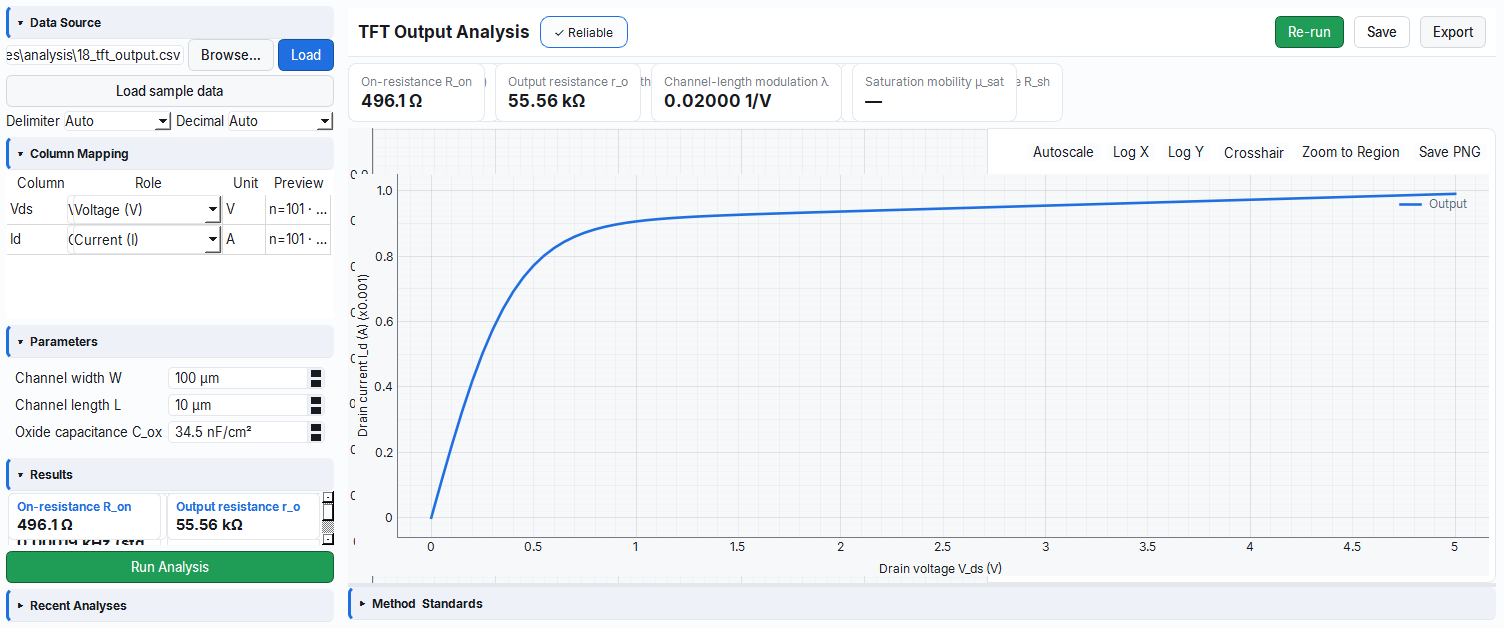
The highest-|V_GS| output curve (I_DS–V_DS) is used; the slope of two different regions of the same curve is taken: the low-V_DS linear region and the high-V_DS saturation region.
- Step: a line is fitted to the low-V_DS linear region (|V| ≤ min(0.5, 0.05·V_max)); the slope dI_DS/dV_DS is taken →
R_on = |1/slope|. - Step: a second line is fitted to the saturation region (|V| ≥ 0.6·V_max) (slope →
r_o = |1/slope|) and this line is carried back to V_DS=0 by extrapolation. - Result: from the slope/intercept of the saturation line,
λ = |slope/intercept|(Early voltageV_A = 1/λ). The linear–saturation transition (knee) is read from the peak of |d²I_DS/dV_DS²|.
A.2 Transfer / On-Off Ratio (Id–Vg)
This is the most fundamental test, considered the transistor's "ID card." We hold the drain voltage fixed, slowly increase the gate voltage (V_GS), and watch when the transistor "turns on," how quickly it turns on, and how much it conducts. It is like turning a dimmer switch and measuring at what point the lamp begins to light and how much brighter it gets.
Physical background: On the logarithmic Id–Vg curve you see three regions. Below threshold (sub-threshold) the channel is only weakly populated; the carrier density depends exponentially on V_GS through Boltzmann statistics, so I_DS increases exponentially and becomes a straight line on the log axis — the slope of this line gives the sub-threshold swing (SS). Above threshold the channel fully forms and I_DS increases linearly/quadratically with V_GS. The flat "floor" at the bottom is the gate/junction leakage (I_off). Thus, on the log curve, the position of the elbow reveals V_th, the steepness reveals SS, and the ceiling/floor ratio reveals I_on/I_off even by eye.
- Why it is done: To determine the transistor's turn-on threshold, switching sharpness, and how well it distinguishes the on/off states.
- What it teaches / measures: V_th = the threshold voltage where the channel turns on; µ (µFE/µ_sat) = how easily carriers flow under the gate field (mobility); SS = the sharpness of switching, the V_GS needed to increase the current by one decade, directly related to the interface trap density; I_on/I_off = the on-off current separation; D_it = the interface trap density derived from SS; ΔV_th (hysteresis) = an indicator of mobile charge/trapping.
- Typical values and their interpretation: SS ~60–100 mV/dec is good (ideal lower bound ≈59.5 mV/dec at 300 K); >300 mV/dec means highly trapped/poor switching; I_on/I_off >10⁶ is a good switch, and 10⁸–10¹⁰ is common in good IGZO TFTs; mobility is on the order of ~1 for a-Si:H, ~10 for IGZO, hundreds of cm²/Vs for poly/crystalline-Si; |ΔV_th| ≪1 V is considered stable.
- Common mistakes / cautions: forgetting the log axis (the sub-threshold region and I_off become invisible); taking I_off from a single noisy point (use the median/deep-off region); skipping the entry of W/L/Cox for mobility (the metric is skipped if 0 is entered); overlooking hysteresis (ΔV_th) in a dual sweep; measuring SS in too wide/wrong a window and finding it larger than it really is.
- Where it is used: baseline characterization and version-to-version quality comparison in TFT/FET development; process monitoring.
Module: measure.transfer · Navigation: Transfer / On-Off Ratio
Purpose: Under a fixed V_DS, it sweeps the gate voltage (V_GS) to measure the transfer characteristic; it extracts the threshold voltage, mobility, sub-threshold swing (SS), on/off ratio, and hysteresis. This is the fundamental measurement of TFT/FET characterization.
What it measures: For each V_GS, I_DS (drain current) and I_GS (gate leakage), at a fixed V_DS.
| Parameter | Unit | Description | Default |
|---|---|---|---|
fixed_vds | V | Fixed drain voltage | 1.0 |
vgs_start / vgs_stop / vgs_step | V | Gate sweep start/stop/step | -5.0 / 5.0 / 0.25 |
mobility_method | — | Linear (g_m, low V_DS) or Saturation (√I_DS) | Linear |
w_um / l_um / cox_nf_cm2 | µm / µm / nF/cm² | Geometry (for µFE, opt.) | 0.0 |
| Common SMU parameters | — | NPLC, compliance, settling, averages, etc. | (common table) |
Computed metrics (transfer_measurement.py):
| Metric | Formula / Method | Unit | Basis |
|---|---|---|---|
| I_on | max |I_DS| | A | — |
| I_off | Median of the deep-off region (V_GS < Vth−2 V; otherwise the lowest 20% of V_GS) — noise-resistant | A | — |
| I_on/I_off | I_on / I_off | — | — |
| g_m / g_m,max | g_m = dI_DS/dV_GS (central difference); g_m,max = max|g_m| | S | — |
| V_th (Linear) | Tangent extrapolation at the peak g_m point: Vth = V_GS* − I_DS*/g_m,max | V | IEC 60747 |
| V_th (Saturation) | x-intercept of the √I_DS–V_GS tangent: Vth = V_GS* − √I_DS*/slope | V | — |
| µFE (Linear) | µFE = g_m,max / ((W/L)·Cox·|V_DS|) | cm²/Vs | — |
| µ_sat (Saturation) | µ_sat = slope²·2L/(W·Cox) (√I_DS slope) | cm²/Vs | — |
| SS (sub-threshold swing) | In a sliding ~1-decade window SS = 1000 / (d log₁₀|I_DS|/dV_GS); the steepest (min) is chosen | mV/dec | — |
| µ0 / V_th,Y (Y-Function) | From the linear fit of Y = I_DS/√g_m: Vth_Y = −intercept/slope, µ0 = slope²/((W/L)·Cox·|V_DS|) | cm²/Vs · V | — |
| D_it (interface trap dens.) | D_it = (Cox/q)·(SS/(kT/q·ln10) − 1) | cm⁻²eV⁻¹ | — |
| ΔV_th (hysteresis) | ΔVth = Vth_forward − Vth_reverse (Dual only) | V | — |
| Hysteresis window | The V_GS difference between the forward/reverse curves at 50%·I_max current | V | — |
kT/q·ln10 ≈ 59.5 mV/dec. If the extracted SS is below this bound, a physical-limit warning is issued and D_it is not computed (it would be negative/meaningless). For SS, if scipy is available, noise correction is done with Savitzky-Golay; otherwise it falls back to the point-by-point method.Plot: Id-Vg linear, Id-Vg logarithmic, and gm-Vg curves (X: V_GS [V]; Y: I_DS [A] or g_m [S]).
The linear (low-V_DS) transfer curve I_DS–V_GS is used; a tangent is drawn at the point where the curve is steepest (peak g_m).
- Step: g_m = dI_DS/dV_GS is computed, the point where it is largest (g_m,max) is found, and a tangent is fitted there.
- Step: the tangent is carried to the x-axis (I_DS=0) by extrapolation; its x-intercept gives the threshold voltage:
V_th = V_GS* − I_DS*/g_m,max. - Result: since the slope of the tangent is g_m,max, the mobility is
µFE = g_m,max / ((W/L)·Cox·|V_DS|). (In the saturation method the same extraction is done with the slope and x-intercept of the √I_DS line.)
The transfer curve is plotted as log I_DS–V_GS (logarithmic transformation); in the sub-threshold region the curve turns into a straight line.
- Step: a line is fitted to an approximately one-decade (10× current) window in the sub-threshold region.
- Step: the slope of this line, d(log₁₀ I_DS)/dV_GS, is taken.
- Result: SS is the inverse of this slope:
SS = ΔV_GS / Δ(log₁₀ I_DS) = 1000/slope(mV/dec). The steepest window (the one giving the smallest SS) is chosen; the physical lower bound at 300 K is ≈59.5 mV/dec.
A.3 Pulsed I-V
Applying continuous voltage heats the device and corrupts the measurement. In this mode the voltage is applied to the device only in very short "pulses," the measurement is taken at the end of the pulse, and then we wait for the device to cool/rest. It is like quickly touching and withdrawing your hand from a hot pan instead of pressing it down continuously — you learn the true temperature without getting burned.
Physical background: Under continuous (DC) bias the device heats up; because heating lowers mobility, I_DS "collapses" over time (the curve bends downward at high V_DS). Also, slow traps capture charge on the ms–s scale and shift the curve. A short pulse (µs–ms) takes the measurement before heat and traps can respond; a long rest lets the device cool and the traps empty. That is why the pulsed curve comes out "steeper/higher" than the DC curve; the difference between the two curves directly gives the magnitude of self-heating and trapping.
- Why it is done: To see the device's "true" behavior by removing self-heating and transient (trap-induced) effects.
- What it teaches / measures: Heating-free I_DS = the device's isothermal (true) current; difference from DC = the self-heating + trapping contribution; duty-cycle effect = the leakage of the pulse/rest ratio into the result.
- Typical values and their interpretation: a duty cycle (pulse_width/period) ≪1 (e.g., 1–10%) provides good isolation; in GaN/power devices a deviation of tens of % between DC and pulsed is a sign of "current collapse" and indicates a serious trap problem.
- Common mistakes / cautions: choosing the pulse width shorter than the instrument's settling time (the current is read before it settles); entering the pulse period shorter than the pulse (gives a validation error); leaving the duty cycle high and heating the device again.
- Where it is used: accurate characterization of power devices and TFTs sensitive to heating/traps.
Module: measure.pulsed_iv · Navigation: Pulsed I-V
Purpose: It measures I_DS while minimizing self-heating and transient effects. At each point the device is excited from a baseline level with a short pulse; the measurement is taken at the end of the pulse, then a rest time is waited.
What it measures: For each (V_GS, V_DS) pulse, the pulsed I_DS and I_GS (time-resolved).
| Parameter | Unit | Description | Default |
|---|---|---|---|
vds_start / vds_stop / vds_step | V | Drain sweep | 0.0 / 5.0 / 0.5 |
vgs_start / vgs_stop / vgs_step | V | Gate step | 0.0 / 5.0 / 1.0 |
pulse_width_s | s | Pulse width (the time during which the measurement is taken) | 0.01 |
pulse_period_s | s | Pulse period (pulse + rest) | 0.1 |
baseline_vds / baseline_vgs | V | Baseline voltages between pulses | 0.0 / 0.0 |
pulse_width_s and pulse_period_s must be positive, and the pulse width cannot be greater than the period; otherwise the measurement does not start. A low duty cycle (width ≪ period) minimizes self-heating.Plot: Id-t (per-pulse time response).
pulse_voltage_and_measure call is simulated; the baseline-pulse-measure-rest cycle is applied.A.4 Q-Pulsed I-V (Q-Pulsed)
In some semiconductors, when voltage is applied for a long time, charge gets caught in "traps" inside and the device's threshold shifts. This mode first holds the device at different quiescent voltages (V_Q) and then performs a fast sweep to capture this shift. It is like dipping a sponge into water for different durations and weighing each time how much heavier it gets (how much charge it has drawn).
Physical background: The device is held at each quiescent voltage (V_Q) for a settling time; during this the traps reach an equilibrium occupancy set by V_Q. Then a fast sweep reads the threshold before the traps empty. Because the captured charge creates an additional electric field in the insulator/interface, V_th shifts; the variation of V_th with V_Q shows how much charge each bias traps. The regular shift of the curves as V_Q increases (horizontal translation) is direct visual evidence of trapping; from the total shift ΔV_th the interface trap density N_t is extracted.
- Why it is done: To measure how much charge trapping shifts the threshold voltage and how sensitive the device is to its bias history.
- What it teaches / measures: ΔV_th,trap = the threshold shift due to quiescent bias (max−min over V_Q); N_t = C_ox·|ΔV_th|/q = the interface/surface trap density; the direction of the V_th(V_Q) curve = implies the trap type (acceptor/donor).
- Typical values and their interpretation: for a good insulator-interface N_t ~10¹⁰–10¹¹ cm⁻² is considered low; ≳10¹² cm⁻² means high trapping and instability; |ΔV_th| is preferably kept below a few hundred mV.
- Common mistakes / cautions: keeping the settling time (quiescent_settle_time_s) short (the traps do not fill, ΔV_th comes out underestimated); entering the C_ox (cox_nf_cm2) value wrong/missing (the N_t scale is corrupted); choosing the turn_on_current threshold close to the noise floor and reading V_th unstably.
- Where it is used: stability/reliability research and assessment of insulator-interface quality.
Module: measure.qpulsed · Navigation: Q-Pulsed I-V
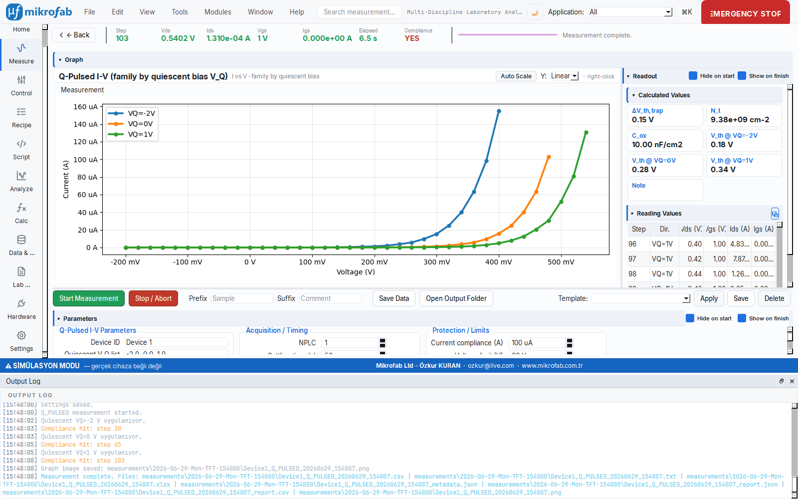
Purpose: With a charge-controlled pulse train, it takes a pulsed I-V sweep at each quiescent voltage point (V_Q). The threshold (V_th) shift at different V_Q values indicates trap loading; from this the interface trap density is estimated.
What it measures: One I-V curve (V, I) for each V_Q; V_th is extracted from each curve.
| Parameter | Unit | Description | Default |
|---|---|---|---|
quiescent_v_list | V (list) | Quiescent bias values | [-2.0, 0.0, 1.0] |
quiescent_settle_time_s | s | Wait after V_Q is applied | 1.0 |
voltage_start / voltage_stop / voltage_step | V | I-V sweep | -0.2 / 1.0 / 0.02 |
pulse_width_s / pulse_period_s | s | Pulse width/period | 1e-4 / 1e-2 |
current_compliance | A | Current limit | 1e-2 |
cox_nf_cm2 | nF/cm² | Capacitance for the N_t computation | 10.0 |
turn_on_current | A | Threshold current for the V_th definition | 1e-6 |
Computed metrics:
| Metric | Formula | Unit |
|---|---|---|
| V_th(V_Q) | The V where I first exceeds turn_on_current in each curve | V |
| ΔV_th,trap | max V_th − min V_th (over V_Q) | V |
| N_t (trap dens.) | N_t = C_ox·|ΔV_th| / q (C_ox = cox_nf×1e-9 F/cm²) | cm⁻² |
Plot: Id-t (pulse response).
V_th_shift = 0.05·V_Q), and I0 is scaled by the appropriate factor; thus N_t comes out consistent.A.5 Hardware Vds–Vgs (Hardware Sweep)
It measures the same output curve, but lets the measurement instrument's (Keithley's) own internal engine perform the sweep loop instead of the software. This way the points are collected at instrument speed without waiting for them one by one. It is like quickly scanning items at a barcode reader instead of reading the shopping list to the cashier one by one.
Physical background: The physical phenomenon measured is the same as A.1; the same curve with a linear→saturation transition emerges on a single channel, so the shape of the curve does not change. The difference is in the timing: the instrument's own internal pipeline (nvbuffer) collects the readings while stepping the voltage with a fixed per-point delay; there is no round-trip to the computer for each point. The cost of this is that each point gets a uniform, short wait, and the ability for flexible averaging/adaptive settling is reduced.
- Why it is done: To collect a large number of points very fast and shorten the measurement time.
- What it teaches / measures: The fast V-I curve of a single channel (the other channel is held fixed); the physical interpretation is the same as the R_on/r_o/λ in A.1, only the data is collected faster.
- Typical values and their interpretation: it collects 100+ points on the order of ms instead of seconds; a per-point delay (delay_s) of ~1 ms is typical; at very low current/high impedance this short delay may not be enough for settling.
- Common mistakes / cautions: leaving the per-point delay too short on a low-current/high-impedance device and taking an unsettled (capacitive) reading; not noticing the trap/heating effect while hysteresis is off; overlooking the discontinuity that autorange transitions create in a fast sweep.
- Where it is used: batch measurement/scanning scenarios where speed matters more than precision.
Module: measure.hw_sweep · Navigation: Hardware Vds–Vgs
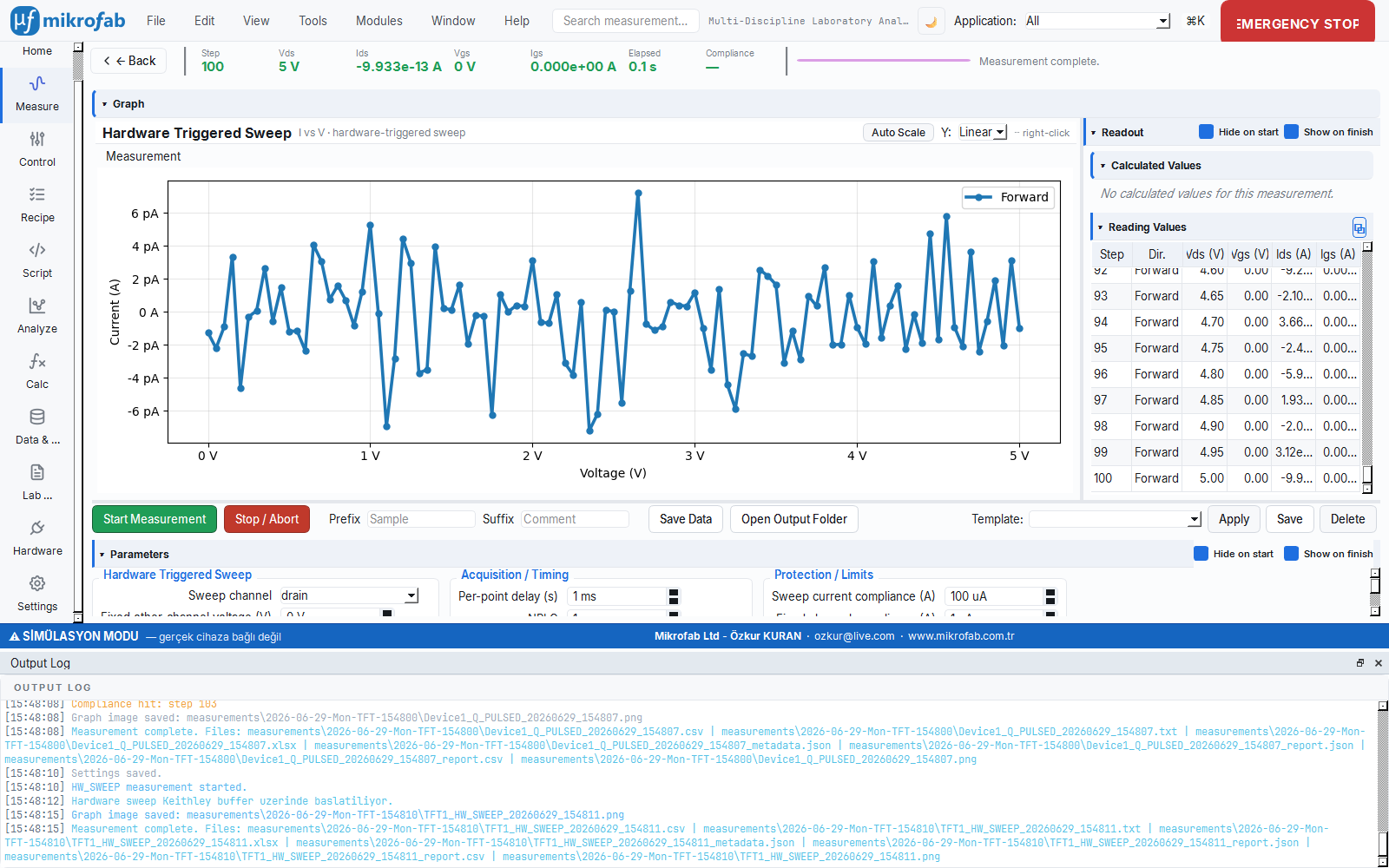
Purpose: On a single channel (drain or gate), it takes a fast output curve using Keithley's own hardware sweep engine (nvbuffer-based list sweep). The software loop does not wait for each point one by one; the data is collected at instrument speed.
What it measures: The voltage-current curve of the swept channel (the other channel is held fixed).
| Parameter | Unit | Description | Default |
|---|---|---|---|
sweep_channel | — | drain or gate (the swept channel) | drain |
fixed_gate_voltage | V | The voltage of the other channel held fixed | 0.0 |
start_voltage / stop_voltage | V | Sweep range | 0.0 / 5.0 |
point_count | — | Number of sweep points (> 1) | 101 |
delay_s | s | Instrument internal per-point delay | 0.001 |
hysteresis | — | Forward + reverse sweep | False |
Plot: Id-Vd (at hardware speed).
run_hardware_linear_voltage_sweep is simulated; the forward and (if selected) reverse sweep buffers are produced.A.6 Hardware TFT I-V (Hardware TFT Sweep)
This is the accelerated version of the output curve family (A.1): at each gate step the instrument's own hardware performs the drain sweep, and the software only manages the gate steps. It is like a conductor in an orchestra who only sets the tempo and lets each section play its own part quickly, rather than dictating each note to every section one by one.
Physical background: The curve family carries the same physics as A.1 (a linear→saturation output curve for each V_GS); the difference is that at each gate step the V_DS sweep is run in a single pass by the instrument's hardware. The software only waits between V_GS steps; the drain sweep finishes at instrument speed at each step, so the full family is collected in a much shorter time. Because the shape of the curves does not change, R_on/r_o/λ are still extracted with the A.1 analysis.
- Why it is done: To collect a complete Id-Vd curve family at hardware speed.
- What it teaches / measures: a fast output curve for each V_GS (the full family at hardware speed); the extracted R_on, r_o, λ, and saturation behavior carry the same meaning as in A.1.
- Typical values and their interpretation: the V_DS sweep per step completes on the order of ms; the settling after a V_GS change (settling_time_s) is critical for the gate to settle.
- Common mistakes / cautions: leaving the settling short after a V_GS change and shifting the first points of each step; insufficient hardware delay at low current; increasing the number of points too much and hitting the instrument buffer limit.
- Where it is used: fast output characterization in multi-device/batch production tests.
Module: measure.hw_tft_sweep · Navigation: Hardware TFT I-V
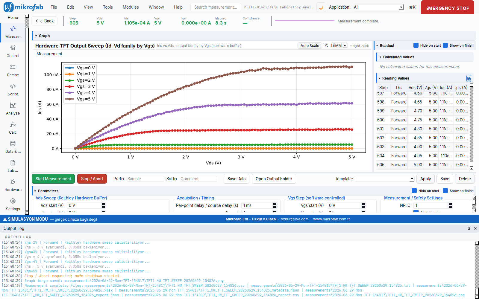
Purpose: The hardware-triggered (buffer-based) version of the output sweep: at each V_GS value, Keithley performs its own internal V_DS sweep; the software manages only the V_GS steps. It provides a complete Id-Vd family at hardware speed.
| Parameter | Unit | Description | Default |
|---|---|---|---|
vds_start / vds_stop | V | Hardware V_DS sweep range | 0.0 / 5.0 |
vds_point_count | — | Number of V_DS points (> 1) | 101 |
vgs_start / vgs_stop / vgs_step | V | Gate step | 0.0 / 5.0 / 1.0 |
delay_s | s | Keithley internal per-point delay | 0.001 |
settling_time_s | s | Wait after a V_GS change | 0.05 |
hysteresis | — | V_DS Forward + Reverse | False |
Plot: Id-Vg (at hardware speed).
B. Diode Modules
All diode-based modules share a common analysis engine (diode_analysis_engine.py). The fundamental physical model is the Shockley diode equation with series (R_s) and shunt (R_sh) resistances:
In forward bias the exponential term dominates: ln(I) = ln(I0) + qV/(nkT). From the slope of this line the ideality factor and the saturation current are extracted:
B.1 Diode I-V
A diode is an "electrical turnstile" that passes current in one direction only. This measurement sweeps the voltage from negative to positive and shows when the diode begins to conduct in the forward direction and how well it blocks in the reverse direction. It is like measuring that a bicycle pedal can be turned easily in only one direction and resists in the other.
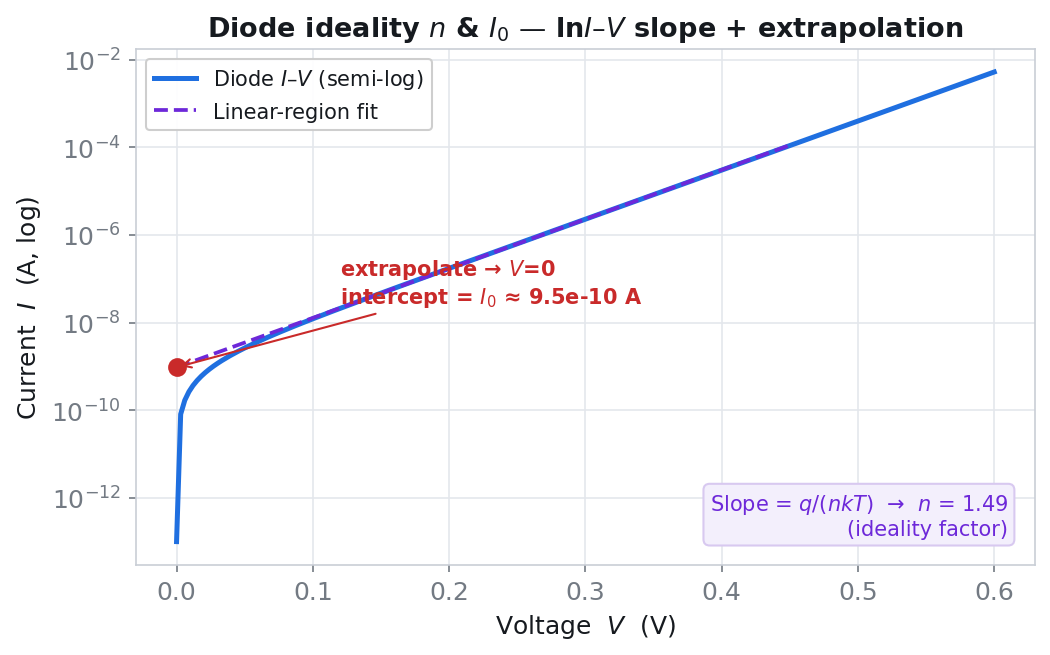
Physical background: In forward bias the current flows exponentially across the junction according to the Shockley equation; on the log(I)–V plot this is a straight line whose slope gives the ideality factor (n). At high current the line "bends" because the series resistance (R_s) takes part of the voltage onto itself. In reverse bias only a small saturation/leakage current (a flat floor) is seen; the turn-on knee is where the exponential arm first exceeds the measurable current. That is why you see a sharp "knee" on the linear plot and a long straight exponential arm on the log plot.
- Why it is done: To understand how "ideally" the diode rectifies, its conduction mechanism, and its losses.
- What it teaches / measures: V_on = turn-on voltage; n (ideality) = conduction mechanism (≈1 diffusion, ≈2 generation-recombination/trap, >2 high-injection, series resistance, or tunneling); I0 = saturation current (material/band gap/surface quality); R_s = series resistance (conduction loss); R_sh = shunt resistance (edge leakage); RR = rectification ratio.
- Typical values and their interpretation: Si pn diode V_on ~0.6 V, Ge ~0.3 V, GaN/LED ~2–3 V; n of 1–2 is good, >2 means trap/leakage dominated; the smaller I0 is (pA–nA), the better; RR ≫10³ is a good rectifier; high R_sh (≫MΩ) is good.
- Common mistakes / cautions: moving the fit range (fit_v_min/fit_v_max) into the high-current region bent by series resistance and inflating n; not using a log axis; hitting compliance and clipping the forward arm; confusing the reverse leakage with the measurement noise floor.
- Where it is used: power/signal diode selection, material quality, and junction quality control.
Module: measure.diode · Navigation: Diode I-V
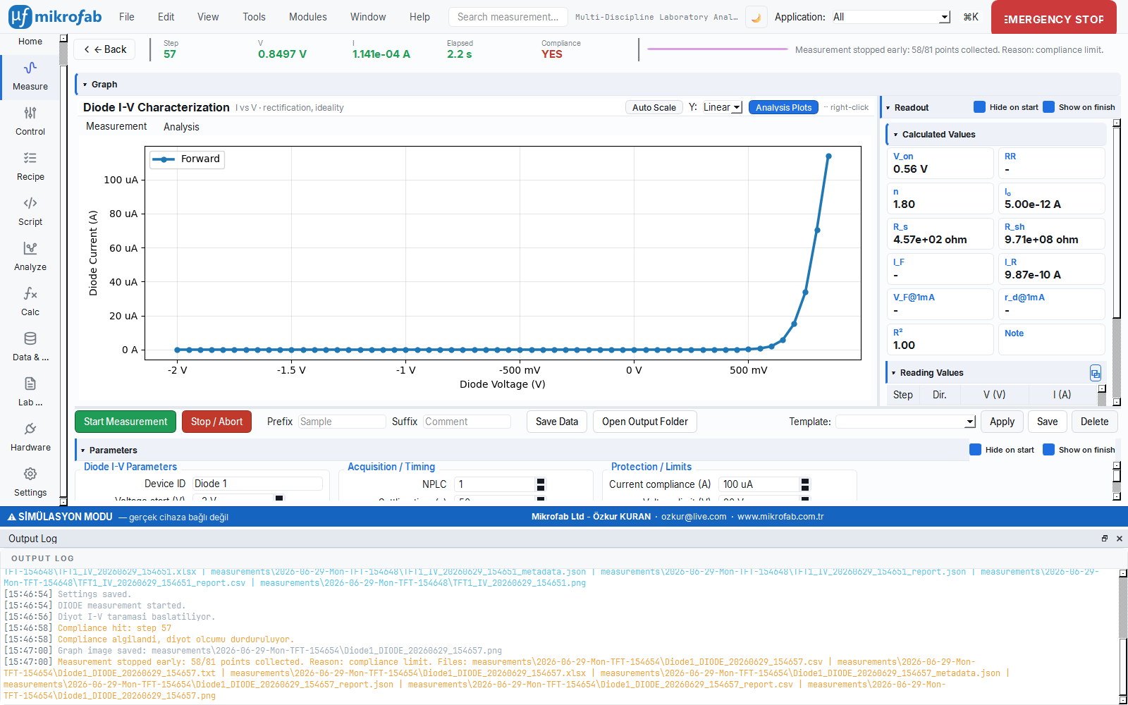
Purpose: With a single-channel SMU it takes the forward+reverse voltage sweep of the diode; it extracts rectification, the ideality factor, the saturation current, and the series resistance.
What it measures: The current I for each V (single channel, V_GS=0).
| Parameter | Unit | Description | Default |
|---|---|---|---|
voltage_start / voltage_stop / voltage_step | V | I-V sweep | -2.0 / 2.0 / 0.05 |
current_compliance | A | Current limit | 1e-3 |
turn_on_current | A | Threshold current for the V_on definition | 1e-6 |
rectification_voltage | V | Rectification-ratio reference voltage ±V_rect | 1.0 |
fit_v_min / fit_v_max | V | ln(I)-V ideality fit range | 0.05 / 0.50 |
Computed metrics:
| Metric | Formula / Method | Unit |
|---|---|---|
| V_on (turn-on) | The V where I first exceeds turn_on_current (interpolation) | V |
| n (ideality) | n = q/(kT·slope), ln(I)-V fit (shunt-corrected, noise-filtered) | — |
| I0 (saturation current) | I0 = exp(intercept) | A |
| R_s (series resistance) | Cheung-1: dV/d(lnI) = R_s·I + nkT/q → slope = R_s | Ω |
| R_sh (shunt resistance) | In the low-V (V ≤ 0) region R_sh = dV/dI | Ω |
| RR (rectification ratio) | RR = |I(+V_rect)| / |I(−V_rect)| | — |
| Forward current / reverse leakage | I@+V_rect / |I@−V_rect| | A |
| V_F@1mA, r_d@1mA | Forward voltage and differential resistance at 1 mA | V / Ω |
| Fit R² | ln(I)-V fit quality | — |
The forward-bias data is plotted as ln I–V (semi-logarithmic transformation); the exponential arm fits a straight line here: ln(I) = ln(I0) + qV/(nkT) (fit range fit_v_min … fit_v_max).
- Step: a line is fitted to the straight portion of the exponential arm (before the high-current region bent by series resistance) and the slope d(ln I)/dV is taken.
- Step: the same line is carried to V=0 by extrapolation; the vertical-axis intercept is
ln(I0). - Result:
n = q/(k·T·slope)(at 300 KkT/q = 0.025852 V);I0 = exp(intercept). The series resistance R_s is extracted from the slope of the Cheung-1 line (dV/d(lnI)–I).
Plot: I-V linear and I-V logarithmic.
B.2 Schottky I-V
A Schottky diode forms from the direct contact of a metal and a semiconductor, and an energy "barrier" arises between them. This measurement is the same as a normal diode sweep; the difference is that the analysis numerically extracts the height of this barrier. It is like electrically measuring the height of the "wall" where two different materials meet.
Physical background: At the metal-semiconductor contact an energy barrier (Φ_B) arises; in forward bias the carriers cross this barrier by thermionic emission. The saturation current I0 depends exponentially on the barrier via the Richardson equation (I0 = A**·T²·Area·exp(−qΦ_B/kT)); from the known A**, T, and area, I0 is solved back to find Φ_B. An ideality n significantly greater than 1 indicates barrier inhomogeneity, image-force lowering, or an interfacial layer; the Cheung method separates the series resistance from the exponential arm. The curve shape is the same as a normal diode's; the extra information comes entirely from the absolute magnitude of I0.
- Why it is done: To determine the quality of the metal-semiconductor contact and the barrier height.
- What it teaches / measures: Φ_B = Schottky barrier height (the rectifying strength of the contact); n = barrier homogeneity/ideality; J0 = I0/Area = area-normalized saturation current density (area-independent comparison); R_s,Cheung = the series resistance separated from the exponential arm.
- Typical values and their interpretation: for Si Schottky, Φ_B ~0.6–0.85 eV is typical; n ~1.02–1.2 means a good/clean contact, ≳1.5 means an inhomogeneous or interfacial contact; the smaller J0 is, the higher the barrier.
- Common mistakes / cautions: not entering the correct material/Richardson constant (A_richardson) (Φ_B is offset); entering the active area (device_area_um2) wrong (J0 and Φ_B shift); leaving the temperature at the default 300 K and not reflecting the real T; moving the ideality fit into the series-resistance bend.
- Where it is used: contact metallurgy research, fast power diodes, and sensor development.
Module: measure.schottky · Navigation: Schottky I-V
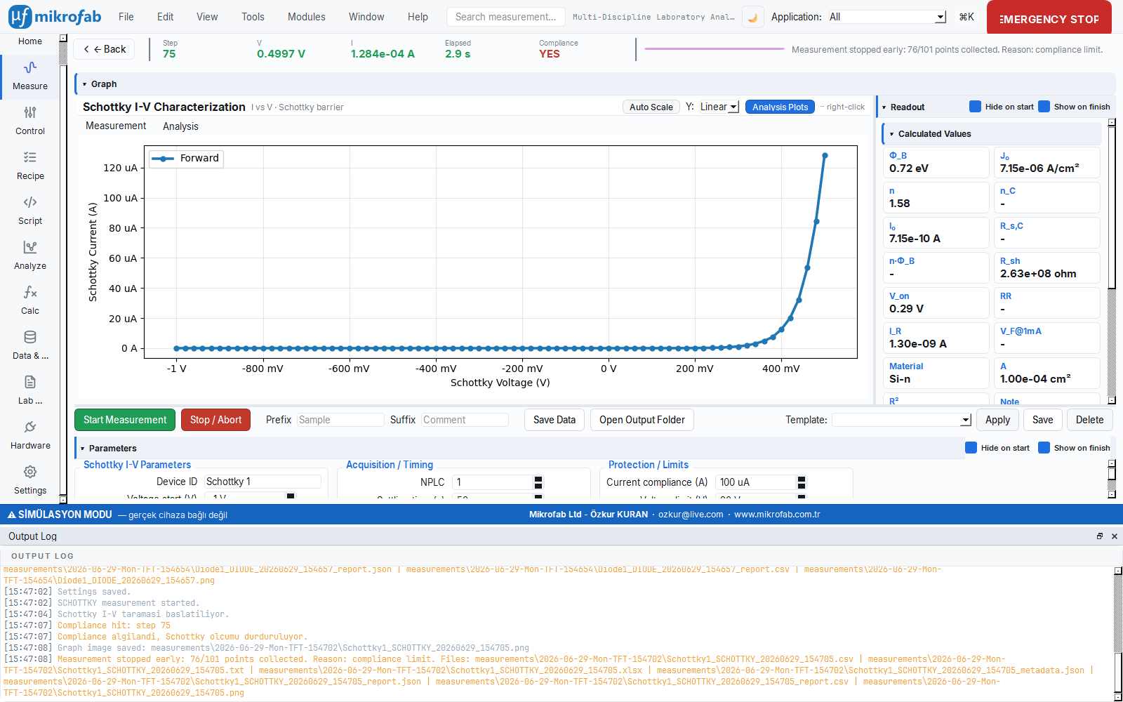
Purpose: The measurement flow is the same as Diode I-V; the difference is in the analysis layer. By providing the active area, the Richardson constant, and the temperature, the Schottky barrier height (Φ_B), the Cheung-1/2 series resistance, and the saturation current density (J0) are extracted from the thermionic emission model.
What it measures: The current I for each V (single channel).
| Parameter | Unit | Description | Default |
|---|---|---|---|
voltage_start / voltage_stop / voltage_step | V | I-V sweep | -1.0 / 1.0 / 0.02 |
current_compliance | A | Current limit | 1e-2 |
rectification_voltage | V | Rectification reference | 0.5 |
fit_v_min / fit_v_max | V | Ideality fit range | 0.10 / 0.40 |
device_area_um2 | µm² | Active area (internal: cm² = ×1e-8) | 10000.0 |
material | — | Si-n / Si-p / GaAs-n / GaN-n / Custom | Si-n |
A_richardson | A/cm²K² | Effective Richardson constant (comes from the material) | 110.0 |
temperature_K | K | Measurement temperature | 300.0 |
cheung_I_min | A | Cheung fit lower bound | 1e-4 |
Richardson constant presets: Si-n 110, Si-p 32, GaAs-n 8, GaN-n 26 A/cm²K².
Computed metrics (in addition to all the diode quantities in B.1):
| Metric | Formula | Unit |
|---|---|---|
| Φ_B (barrier height) | Φ_B = (kT/q)·ln(A**·T²·Area / I0) | eV |
| J0 (saturation current density) | J0 = I0 / Area | A/cm² |
| n_Cheung, R_s,Cheung1 | Cheung-1 intercept/slope | — / Ω |
| R_s,Cheung2, n·Φ_B | Cheung-2: H(I) = V − nVt·ln(I/(A**T²Area)) = R_s·I + n·Φ_B | Ω / eV |
The measurement flow is the same as the diode: the forward arm is transformed into the ln I–V line. n and I0 come from this line, while Φ_B is computed from I0 via the Richardson (thermionic emission) relation.
- Step: the slope of the ln I–V line →
n = q/(k·T·slope); extrapolating the line to V=0 →I0 = exp(intercept). - Step: the active area (Area), temperature (T), and Richardson constant (A**) are entered.
- Result: the barrier height is extracted not from the plot but from I0:
Φ_B = (kT/q)·ln(A**·T²·Area / I0). For the series resistance the Cheung method (the slope of the dV/d(lnI)–I line) is used.
Plot: I-V logarithmic.
I0 = A**·T²·Area·exp(−Φ_B/Vt), n=1.6, R_s=30 Ω); the analysis recovers this Φ_B.B.3 Reverse Recovery (trr)
When a diode transitions from conduction to blocking, it conducts current in the reverse direction for a moment — because it takes time for the stored charge inside it to discharge. This measurement suddenly reverses the diode and records, on the time axis, how long it takes for this transient current to die out. It is like using a stopwatch to measure how long the water in a pipe keeps dripping after you close the faucet.
Physical background: During forward conduction, minority-carrier charge (Q) is stored in the junction region of a pn diode. When the device is suddenly reversed, this charge must be swept out and discharged before the diode can block; during this a large reverse current flows, then decays exponentially with the minority-carrier lifetime (τ). Because a Schottky diode operates with majority carriers, it stores almost no minority charge; therefore its recovery is very fast. The negative current dip and the exponential tail that follows it, which you see on the plot, are a direct picture of this charge discharge.
- Why it is done: To measure how fast the diode can switch (its suitability for high frequency).
- What it teaches / measures: t_rr = reverse recovery time (switching speed); I_rr = peak reverse current; Q_rr = I_F·τ = recovery charge (the total charge discharged); τ = minority-carrier lifetime (from the exponential fit).
- Typical values and their interpretation: for a fast/Schottky diode t_rr is on the order of ns (τ ~10 ns); for a standard pn rectifier ~µs (τ ~µs–10 µs); a small Q_rr / I_rr / t_rr means low switching loss at high frequency.
- Common mistakes / cautions: using the dimensionally incorrect formula
2·Q_rr/I_rr²for τ (as explained in the scientific note alongside, it is wrong; τ comes from the exponential fit); leaving the sampling interval (sample_interval_s) too coarse and missing the peak/decay; not specifying the i_rr_fraction definition when reporting t_rr. - Where it is used: switching power supplies and high-speed rectifier design.
Module: measure.rev_recovery · Navigation: Reverse Recovery (trr)
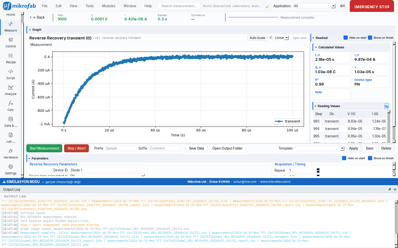
Purpose: It measures, in the time domain, the transient reverse-current decay after sudden switching from a forward bias current (I_F) to a reverse voltage (V_R); it extracts the reverse recovery time, an indicator of switching speed.
What it measures: The transient current I(t) in a time series (the x axis is time).
| Parameter | Unit | Description | Default |
|---|---|---|---|
i_forward | A | Forward bias current (I_rr reference) | 1e-3 |
v_reverse | V | Reverse step voltage | -1.0 |
t_forward_s | s | Forward bias duration | 1e-3 |
t_measure_s | s | Measurement window | 1e-4 |
sample_interval_s | s | Time resolution | 1e-7 |
i_rr_fraction | — | t_rr definition: this fraction of I_rr | 0.1 |
device_type_hint | — | Schottky / PN (mock τ selection) | PN |
Computed metrics:
| Metric | Formula | Unit |
|---|---|---|
| I_rr | max |I(t)| (peak reverse current) | A |
| Q_rr | Q_rr = ∫|I(t)| dt (trapezoidal) | C |
| τ (minority-carrier lifetime) | From the ln|I|–t exponential decay fit τ = −1/slope | s |
| t_rr | The instant when |I| drops to i_rr_fraction·I_rr (interpolation) | s |
τ ≈ 2·Q_rr/I_rr² found in some sources is dimensionally incorrect (C/A² = s/A). The correct relations in the exponential model are Q_rr = I_F·τ and t_rr = τ·ln(1/i_rr_fraction); therefore τ is extracted from the exponential fit.Plot: I-t (transient).
I(t) = −I_F·exp(−t/τ) + small noise; τ is selected from the type hint (Schottky ≈ 10 ns, PN ≈ 10 µs).C. Resistivity / Resistance Modules (TFT / Thin Film)
C.1 Four-Point Probe Resistivity
It measures "how conductive" a thin film is. Four probes are used: current is driven through the outer two, and voltage is read from the inner two — so the resistance of the cables and contact points does not enter the measurement. It is like measuring the true length of a road without counting the toll booths at its beginning and end.
Physical background: Current is driven through the outer probes and voltage is read from the inner probes; because no current flows through the voltage probes, their contact/cable resistance does not enter the measurement as an IR drop — this is the entire power of the 4-point method. In a thin layer (thickness ≪ probe spacing) the current spreads in two dimensions, and the geometric factor π/ln2 ≈ 4.5324 converts the measured resistance into the sheet resistance (R_s). If the film thickness is known, the resistivity is ρ = R_s·t. The V-I points should trace a straight line passing through the origin; curvature or offset means a poor contact/noise.
- Why it is done: To measure the conduction quality of a coating/film free of contact resistance.
- What it teaches / measures: R_s = sheet resistance (Ω/sq, a thickness-independent film indicator); ρ = resistivity (the material's intrinsic resistance); σ = 1/ρ = conductivity.
- Typical values and their interpretation: metal contact films (Al/Au) ~mΩ–tens of Ω/sq; transparent conductors like ITO ~10–100 Ω/sq; doped/weak semiconductor films kΩ–MΩ/sq; metals' resistivity is ~10⁻⁶ Ω·cm, much higher in semiconductors.
- Common mistakes / cautions: overlooking the thin/thick regime distinction (t < s/2 is thin) and using the wrong ρ formula; forgetting that if the thickness (film_thickness_nm) is not entered, only R_s is produced; ignoring fit R²<0.99 (poor contact/noise); measuring too close to the sample edge and falling into the edge effect.
- Where it is used: quality control and material comparison in thin-film/coating production.
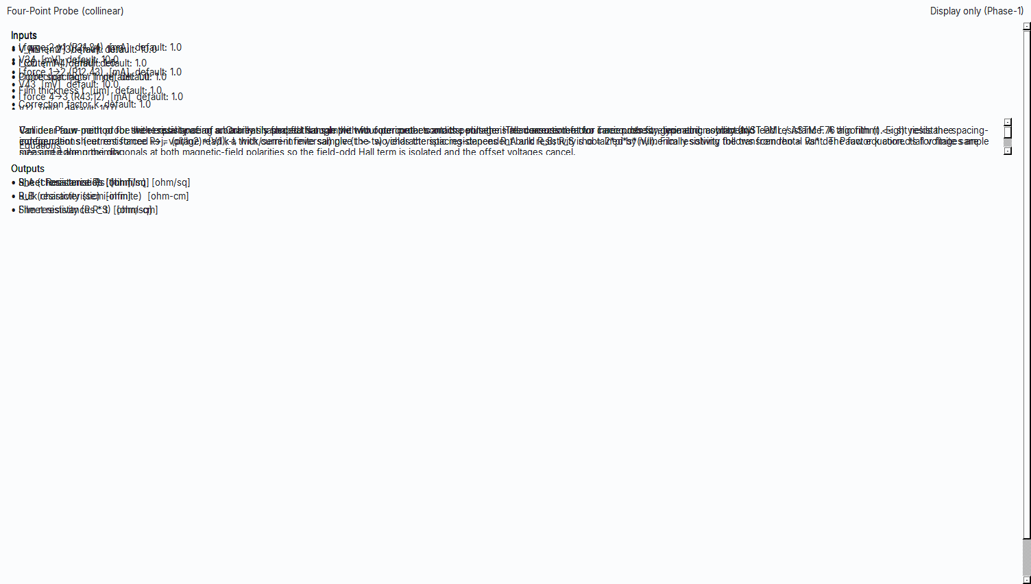
Module: measure.four_point · Navigation: Four-Point Probe Resistivity
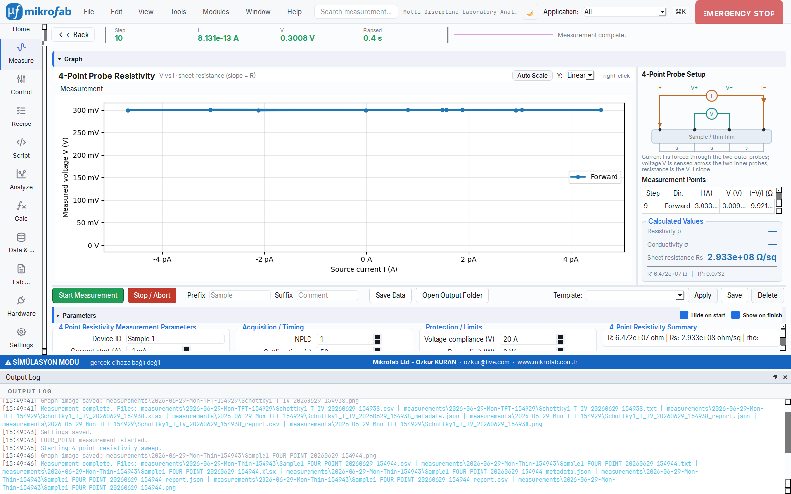
Purpose: With a collinear (equally-spaced) 4-point probe it measures sheet resistance and resistivity. A current series is driven through the outer probes (1 and 4), and a 4-wire voltage is read from the inner probes (2 and 3); this excludes the cable/contact resistance from the measurement.
What it measures: The voltage measured against the driven current series; R = dV/dI.
| Parameter | Unit | Description | Default |
|---|---|---|---|
current_start / current_stop / current_step | A | Source current sweep | -1e-3 / 1e-3 / 2e-4 |
probe_spacing_in | in | Probe spacing (collinear, equal) | 0.1 |
film_thickness_nm | nm | Film thickness (0 = unknown → R_s only) | 0.0 |
voltage_limit | V | Current-source voltage compliance | (common) |
Computed metrics (geometric factor π/ln2 ≈ 4.5324):
| Metric | Formula | Unit |
|---|---|---|
| R | Slope of the V-I linear fit (dV/dI) | Ω |
| R_s (sheet resistance) | R_s = (π/ln2)·R ≈ 4.5324·R | Ω/sq |
| ρ (resistivity) — thin film | t < s/2: ρ = R_s·t | Ω·cm |
| ρ (resistivity) — thick sample | t ≥ s/2: ρ = 2π·s·R (bulk formula) | Ω·cm |
| σ (conductivity) | σ = 1/ρ | S/cm |
Unit conversion: in→cm ×2.54; nm→cm ×1e-7. The regime field is reported as thin / bulk / sheet_only.
The 4-wire voltage measured against the driven current series is plotted; the slope of this line gives the resistance (because no current flows through the voltage probe, the cable/contact resistance is excluded from the measurement).
- Step: a line is fitted to the V–I points; the slope R = dV/dI is taken.
- Step: the geometric factor of the collinear geometry is applied:
R_s = (π/ln2)·R ≈ 4.5324·R(Ω/sq). - Result: if the thickness is known, in the thin regime (t < s/2) the resistivity is
ρ = R_s·t, conductivityσ = 1/ρ.
Plot: R readings (V-I points). The interface also includes a visual panel showing the probe arrangement.
C.2 Van der Pauw / Hall
It measures the resistance of a small, irregularly shaped sample from four contacts placed on its edge, in different combinations. If a magnetic field is added on top (the Hall effect), the type, number, and mobility of the charge carriers inside it are also revealed. It is like watching objects floating in a river to figure out in which direction, at what speed, and at what density the water flows.
Physical background: In the van der Pauw method, the resistance is measured in two directions (Ra, Rb) from the four contacts on the edge of an arbitrarily shaped thin sample; when these are inserted into the van der Pauw relation, the sheet resistance (R_s), independent of the sample shape, is extracted. In the Hall measurement, under a magnetic field (B) the Lorentz force pushes the carriers to the side and a transverse Hall voltage (V_H) arises; the sign of V_H gives the carrier type (N/P), and its magnitude gives the carrier density. Combined with R_s, the mobility (µ) is found. That is why Ra≈Rb (high homogeneity) and a clear V_H sign are the first indicators of the measurement's reliability.
- Why it is done: To determine the material's conductivity and the type/density/mobility of the carriers inside it together.
- What it teaches / measures: R_s/ρ = sheet resistance/resistivity; carrier type = the sign of R_H (R_H<0 N-Type, >0 P-Type); n = 1/(|R_H|·q) = carrier density; µ = |R_H|/ρ = mobility; n_s = sheet carrier density; Homogeneity = the Ra≈Rb consistency check.
- Typical values and their interpretation: homogeneity >95% (Ra≈Rb) is considered good; in films like IGZO µ ~1–20 cm²/Vs, in crystalline Si hundreds, in GaAs thousands of cm²/Vs; the carrier density varies between 10¹⁵–10²⁰ cm⁻³ depending on doping.
- Common mistakes / cautions: entering the thickness (thickness_nm) wrong (the ρ and n scale is corrupted); neglecting the B calibration/duty value (R_H and µ shift); not noticing that the contacts are non-ohmic; ignoring that the VdP assumption breaks down when the homogeneity is ≪95%.
- Where it is used: new semiconductor material research and doping verification.
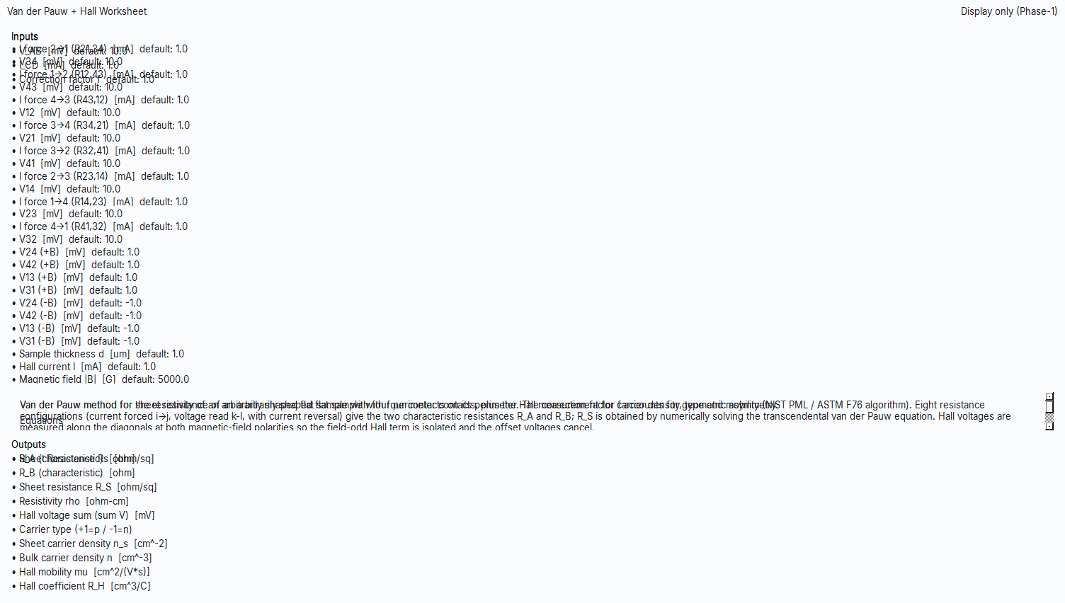
Module: measure.vdp · Navigation: Van der Pauw / Hall
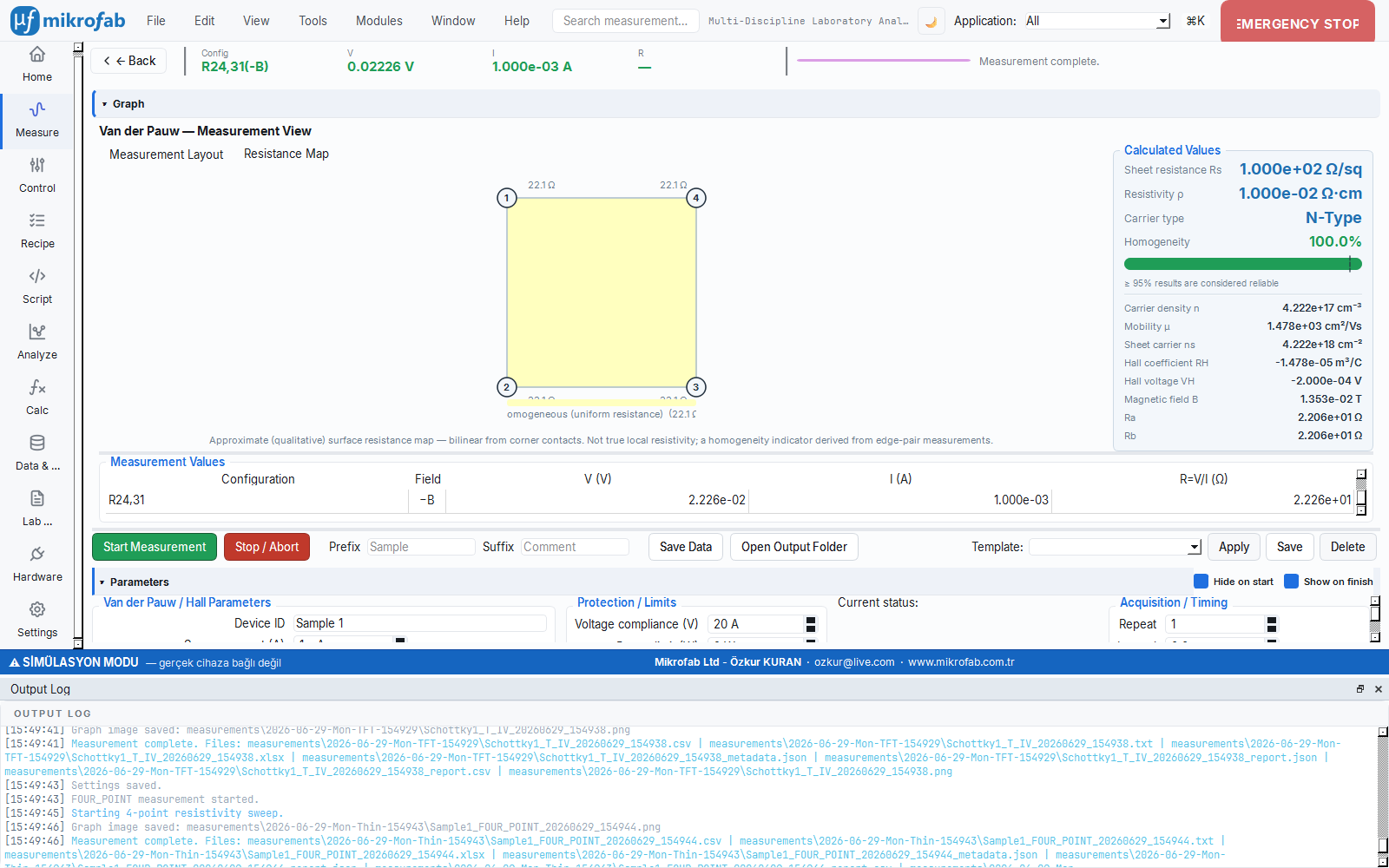
Purpose: Using the van der Pauw method, it measures the sheet resistance and resistivity of an arbitrarily shaped thin sample, and optionally, with a Hall measurement, the carrier type/density and mobility. It operates in single-SMU current-source mode; on a 16-relay switch matrix card, 8 contact configurations are selected in sequence.
What it measures: In each relay configuration a fixed current is driven and the voltage is read (R = V/I). 8 configs → Ra (first 4) and Rb (last 4). When Hall is on, 4 more configs each are measured in the +B/−B field.
| Parameter | Unit | Description | Default |
|---|---|---|---|
source_current | A | Driven fixed current | 1e-3 |
voltage_limit | V | Voltage compliance | 5.0 |
thickness_nm | nm | Film thickness (for resistivity/Hall) | 1000.0 |
magnetic_field_duty | 0..255 | Switch matrix PWM duty cycle (Hall) | 150 |
enable_hall | — | Whether to perform the Hall measurement (+B/−B) | True |
per_point_delay_s | s | Measurement delay after relay/current setting | 0.1 |
mock_inhomogeneous | — | (Mock only) inhomogeneous film simulation | False |
Computed metrics:
| Metric | Formula | Unit |
|---|---|---|
| Ra / Rb | Average of the relevant 4 configs | Ω |
| Homogeneity | (1 − |Ra−Rb|/avg)·100 | % |
| R_s (sheet resistance) | R_s = (π/ln2)·((Ra+Rb)/2) | Ω/sq |
| ρ (resistivity) | ρ = R_s·t | Ω·cm |
| V_H (Hall voltage) | Average of (V₊−V₋)/2 of the matching +B/−B configs | V |
| R_H (Hall coefficient) | R_H = V_H·t / (I·B) | m³/C |
| n (carrier dens.) | n = 1/(|R_H|·q) (×1e-6 → cm⁻³) | cm⁻³ |
| Carrier type | R_H < 0 → N-Type, R_H > 0 → P-Type | — |
| µ (mobility) | µ = |R_H|/ρ_SI · 1e4 | cm²/Vs |
| n_s (sheet carrier dens.) | n_s = n·t·1e7 | cm⁻² |
Magnetic field calibration: B = (duty/255)·0.023 T (duty=255 ≈ 23 mT).
18F12F11F5F, +B<duty>) are specific to the user's 16-relay van der Pauw card and are preserved exactly. If the homogeneity is below 95%, a warning is issued.Here, instead of a single plot slope, the resistances measured in different contact configurations and the Hall voltage are inserted into the van der Pauw relations (formula-based extraction).
- Step: the resistance averages in the two directions (Ra, Rb) are taken →
R_s = (π/ln2)·((Ra+Rb)/2), resistivityρ = R_s·t. - Step: the Hall voltage
V_H = (V₊−V₋)/2is measured; the Hall coefficientR_H = V_H·t/(I·B)(its sign gives the carrier type: R_H<0 N-Type). - Result: carrier density
n = 1/(|R_H|·q), mobilityµ = |R_H|/ρ.
Plot: VDP map (config-based resistances + surface resistance map).
mock_inhomogeneous=True, the resistance is varied across configs with contact weights (homogeneity <100%, a meaningful surface gradient).C.3 Kelvin 4-Wire Resistance
This is the way to measure very small resistances accurately. The wires carrying the current and the wires reading the voltage are separated; this way the resistance of the cables and contacts is not added to the result. With an optional 2-wire measurement for comparison, you can extract the contact resistance on its own. It is like weighing the packaging separately and subtracting it to learn a package's net weight.
Physical background: The current-carrying (Force) and voltage-reading (Sense) wires are separate; because almost no current flows through the Sense wire, the IR drops across the cable/contact do not enter the measurement, and the V/I read gives the true device resistance. The 2-wire measurement, on the other hand, also includes the contact+cable resistance; the difference between the two measurements directly gives the contact resistance (R_contact). That is why the 4-wire curve comes out "steeper" (lower R) while the 2-wire curve is always either the same or flatter; the difference between them is a measure of contact quality.
- Why it is done: To measure the true device/series resistance free of cable and contact effects.
- What it teaches / measures: R_4wire = the true device/series resistance (excluding cable+contact); R_2wire = the total resistance (including contact); R_contact = R_2wire − R_4wire = the contact resistance on its own; V_F@1mA = a reference operating voltage.
- Typical values and their interpretation: in a good ohmic contact R_contact ≪ R_device (mΩ–Ω); if R_contact approaches R_4wire, the contact is problematic; high NPLC suppresses noise in low-resistance measurements.
- Common mistakes / cautions: connecting the Force/Sense terminals to the wrong point and rendering the 4-wire ineffective; measuring a low resistance at low NPLC and drowning it in noise; turning off the 2-wire comparison (compare_2wire) and never seeing R_contact.
- Where it is used: characterization of low-resistance contacts/conductors and contact quality inspection.
Module: measure.kelvin · Navigation: Kelvin 4-Wire Resistance
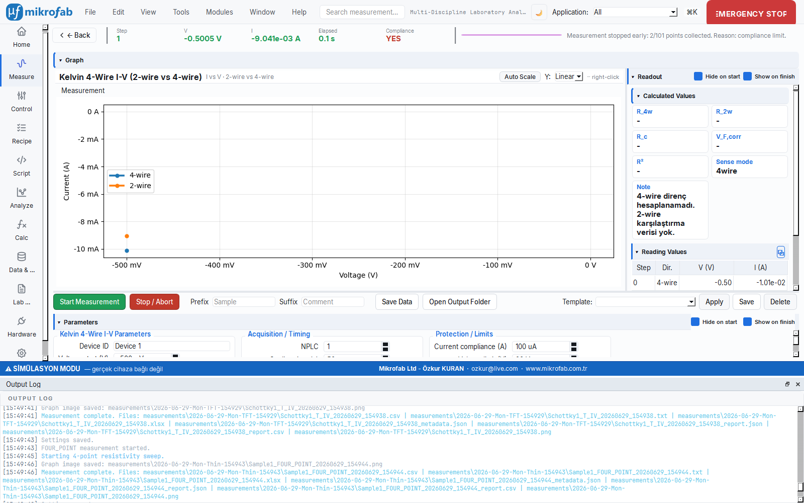
Purpose: With a 4-wire (Force/Sense) measurement it measures the true device/series resistance, excluding the cable and contact resistance. With an optional 2-wire comparison the contact resistance is extracted.
What it measures: The current against a voltage sweep; in each mode R = dV/dI.
| Parameter | Unit | Description | Default |
|---|---|---|---|
voltage_start / voltage_stop / voltage_step | V | I-V sweep | -0.5 / 0.5 / 0.01 |
current_compliance | A | Current limit | 0.1 |
nplc | — | High NPLC for low-current sensitivity | 10.0 |
settling_time_s | s | Settling time | 0.1 |
sense_mode | — | 2wire / 4wire | 4wire |
compare_2wire | — | Also perform a 2-wire comparison sweep | True |
Computed metrics:
| Metric | Formula | Unit |
|---|---|---|
| R_4wire | Slope of the 4-wire V-I fit (true series resistance) | Ω |
| R_2wire | 2-wire total resistance | Ω |
| R_contact | R_2wire − R_4wire | Ω |
| V_F@1mA | The voltage at 1 mA on the 4-wire curve (interp) | V |
| Fit R² (4-wire) | Linear fit quality | — |
A separate line is fitted to each of the 4-wire and (if present) 2-wire V–I sweeps; the difference between the resistances read from the two slopes gives the contact resistance.
- Step: the slope of the 4-wire V–I points → the true series resistance
R_4wire = dV/dI(excluding cable/contact). - Step: the slope of the 2-wire sweep →
R_2wire(the total resistance including contact). - Result: the contact resistance is the difference of the two measurements:
R_contact = R_2wire − R_4wire.
Plot: R-I.
C.4 Probe Station I-V
On a probe station, needle-tipped probes are brought into contact with the device's contact points; this mode selects two probes through the switch matrix and extracts the resistance by performing a simple voltage-current sweep. It is like touching the multimeter leads to two points on a circuit board and reading the resistance; here the software does the lead selection.
Physical background: The voltage is swept between two probes and the current is read; in an ohmic structure the I-V is a straight line through the origin, and its slope gives the conductance (G = dI/dV). Because this is a 2-wire measurement, the probe/contact resistance is included in the result. If the curve deviates from linearity (bending), it indicates that the contact or the device is not ohmic; this is a fast "is it working / is the contact good" check on a probe station.
- Why it is done: To take a fast 2-wire resistance/conductance measurement on a micromanipulator probe station.
- What it teaches / measures: R = the device's resistance; G = dI/dV = its conductance; linearity (R²) = an indicator of whether the contact/device is ohmic.
- Typical values and their interpretation: R² ≈1 means clean ohmic behavior; low R² means curvature/contact problem; the measured R is the sum of the true device + probe/contact resistance.
- Common mistakes / cautions: because it is 2-wire, mistaking the contact contribution for the true device resistance at small resistances (switch to Kelvin if needed); selecting the same probe as both Force HI and Force LO (validation error); hitting compliance and clipping the curve.
- Where it is used: fast electrical checking of individual devices/structures on a wafer.
Module: measure.probe_iv · Navigation: Probe Station I-V
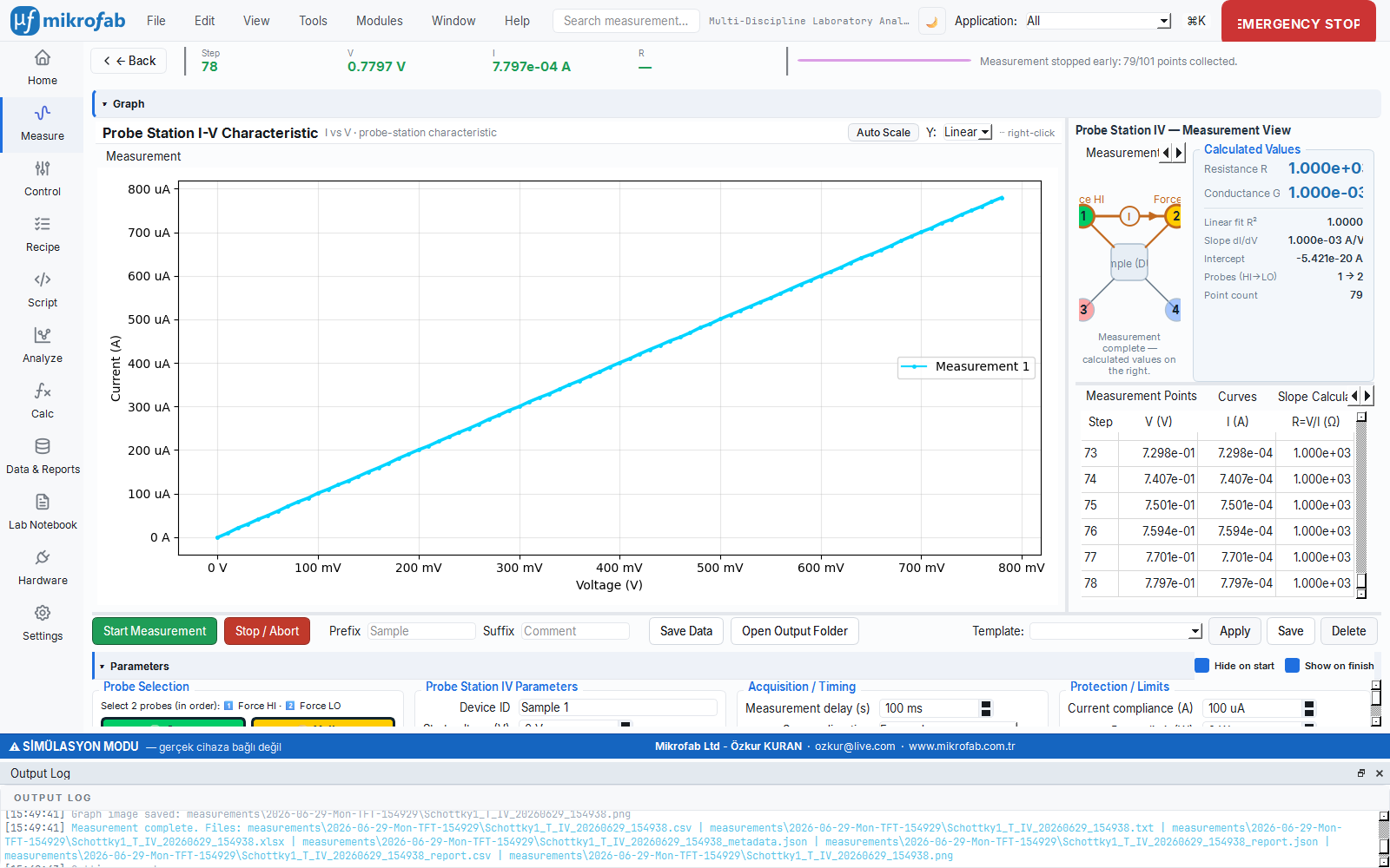
Purpose: The switch matrix card selects 2 of 4 probes (Force HI / Force LO); the SMU performs a 2-wire I-V sweep in voltage-source mode and extracts the resistance. It is suitable for use with a micromanipulator probe station.
What it measures: The current against a voltage sweep; G = dI/dV, R = 1/G.
| Parameter | Unit | Description | Default |
|---|---|---|---|
start_voltage / stop_voltage / step_voltage | V | I-V sweep | 0.0 / 1.0 / 0.01 |
current_compliance | A | Current limit | 0.1 |
delay_s | s | Per-point wait | 0.1 |
force_hi_probe | 1..4 | Force HI probe | 1 |
force_lo_probe | 1..4 | Force LO probe | 2 |
Computed metrics:
| Metric | Formula | Unit |
|---|---|---|
| G (conductance) | I = slope·V + intercept; slope = dI/dV | S |
| R (resistance) | R = 1/G | Ω |
| Slope / intercept / R² | Linear fit | A/V · A · — |
Plot: I-V. The interface includes a visual panel showing the probe→pin map.
D. Reliability Modules
D.1 Bias Stress / Transient
It applies a constant voltage/current to the device and monitors how its current "drifts" over time. In a good device the current should stay constant; if there is drift, the device fatigues. It is like holding a spring at a certain tension and observing whether it loosens over time.
Physical background: Under constant bias, charge is slowly trapped in the insulator/interface (and self-heating contributes); this causes the drain current to drift over time — generally a slow decrease or increase. The shape of the I_DS(t) curve reflects the trapping kinetics: in a stable device the line stays flat, and the larger and more sustained the drift, the more unstable the device. This is the raw appearance of the threshold shift over time.
- Why it is done: To see how stable the device remains under continuous operation.
- What it teaches / measures: The magnitude and direction of I_DS(t) drift = a measure of stability; in current mode the shift in the required voltage indirectly implies the threshold shift.
- Typical values and their interpretation: a drift below a few % over the test duration is considered stable; a shift of tens of % is a sign of significant trapping/degradation.
- Common mistakes / cautions: keeping the test duration (total_duration_s) too short relative to the trap time constants and missing the drift; leaving the sampling interval coarser than necessary; not supporting it with a pulsed measurement to separate self-heating from trapping.
- Where it is used: basic reliability/stability screening and fast elimination tests.
Module: measure.bias_stress · Navigation: Bias Stress / Transient
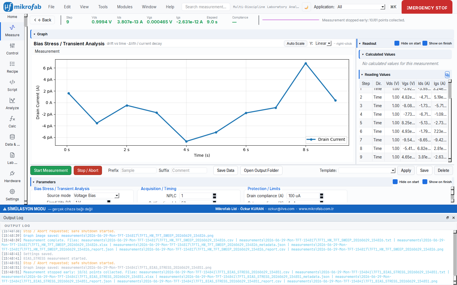
Purpose: It records the drift of the drain current over time under a constant bias (voltage or current). It is a basic reliability/stability test.
What it measures: The I_DS(t) and I_GS(t) time series at fixed intervals.
| Parameter | Unit | Description | Default |
|---|---|---|---|
source_mode | — | Voltage Bias / Current Bias | Voltage Bias |
fixed_vds / fixed_vgs | V | Fixed drain/gate voltages | 1.0 / 0.0 |
drain_current_set | A | (In current mode) fixed drain current | 1e-6 |
total_duration_s | s | Total stress duration | 60.0 |
sample_interval_s | s | Sampling interval | 1.0 |
plot_quantity | — | Quantity to be plotted | Drain Current |
Plot: Id-t.
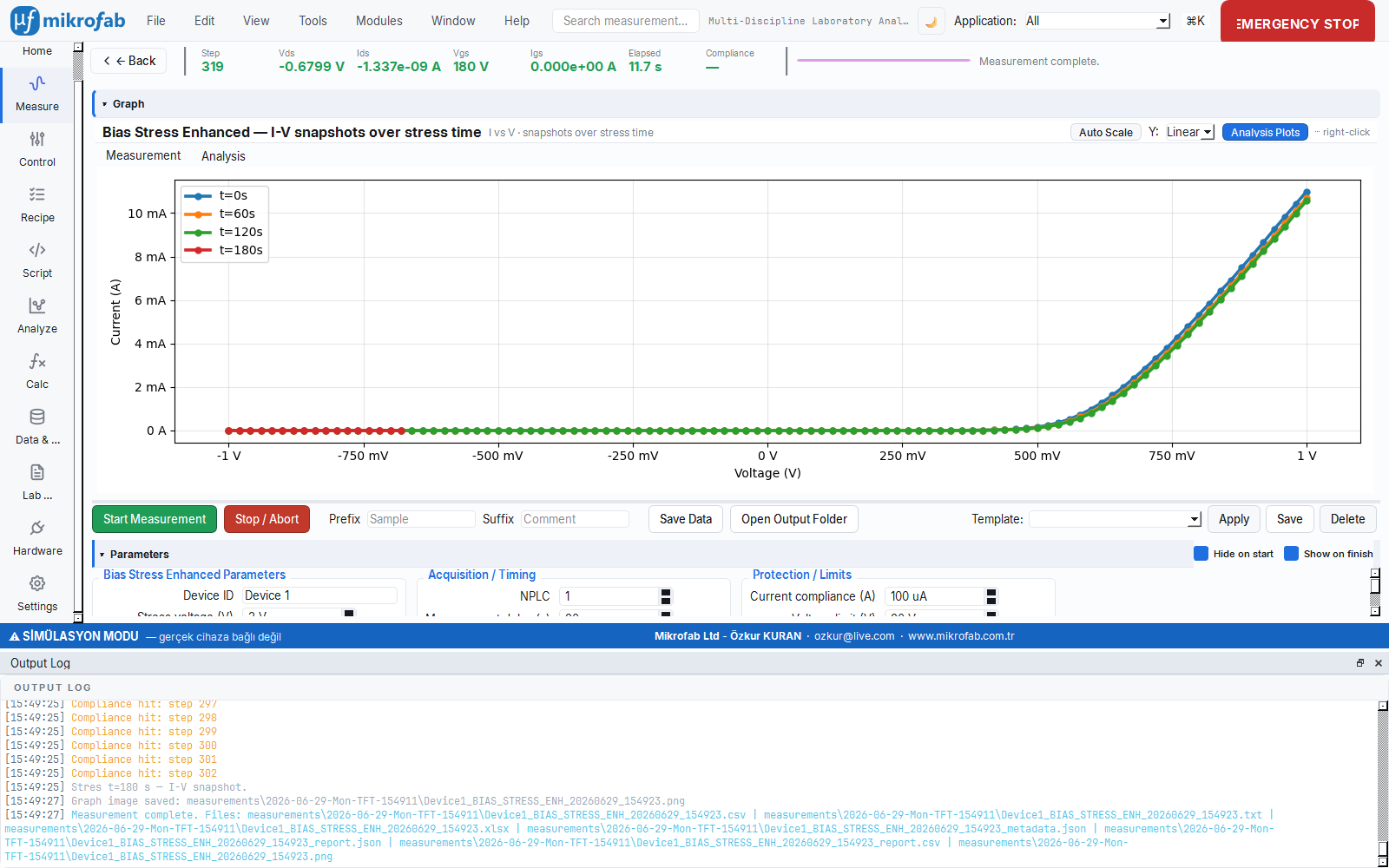
D.2 Bias Stress (Enhanced)
This is the "diagnostic" version of the previous test: while stress is ongoing, it takes fast I-V snapshots at certain intervals, extracts the threshold from each, and models the threshold shift against time to predict when the device will "fail." It is like regularly measuring a tire's wear and computing after how many km it will be worn out.
Physical background: Under stress, the threshold voltage shifts in a power-law (or stretched-exponential) form of time as the traps fill. Periodic I-V snapshots track V_th(t); the ΔV_th(t)=A·t^p curve is fitted and extrapolated to a failure criterion (vth_fail) to predict the mean time to failure (MTTF). The exponent p implies the trapping mechanism (diffusion- or capture-limited); that is why it is not a single snapshot but the trend of the snapshot sequence over time that is meaningful.
- Why it is done: To model the time course of the threshold shift and predict the device's lifetime.
- What it teaches / measures: ΔV_th(t) = the threshold shift trajectory; p = the stress exponent (mechanism indicator); A = the shift coefficient; MTTF = lifetime/time-to-failure prediction; drift rate = the V_th–log₁₀(t) slope (V/decade).
- Typical values and their interpretation: p ~0.2–0.6 is typical for trapping-limited processes (p=0.5 in mock); the larger MTTF is, the more durable; the more slowly |ΔV_th| reaches the failure threshold (e.g., 0.1 V), the more stable the device.
- Common mistakes / cautions: expecting the activation energy E_a at a single temperature (it is extracted only with multi-temperature stress, returns N/A at a single T); doing the fit in log-log and inflating the small-t noise (it must be fitted in linear space); over-extrapolating a long-term MTTF from too short a total stress.
- Where it is used: lifetime/reliability qualification and process improvement comparisons.
Module: measure.bias_stress_enh · Navigation: Bias Stress (Enhanced)
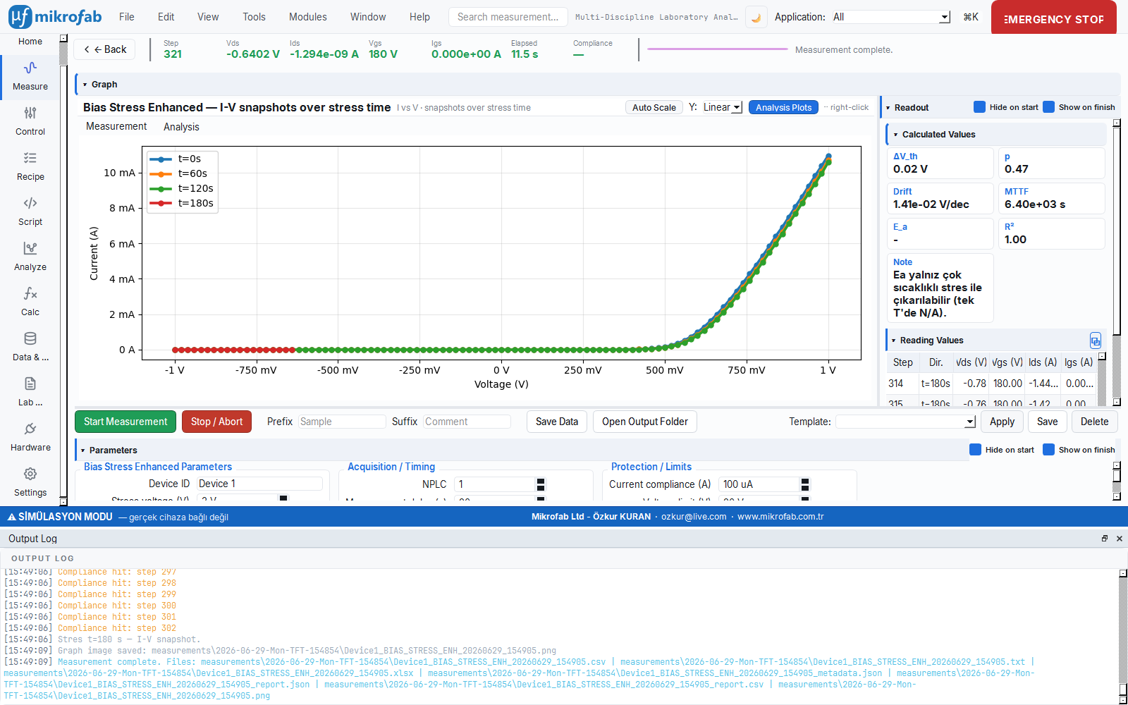
Purpose: While stress is being applied, it takes fast I-V snapshots at certain intervals; from each snapshot it extracts V_th(t), n(t), I0(t). A power law is fitted to the threshold shift and the time to failure (MTTF) is extrapolated.
What it measures: A sequence of I-V snapshots against time; V_th/n/I0 from each.
| Parameter | Unit | Description | Default |
|---|---|---|---|
stress_voltage | V | Applied stress voltage | 2.0 |
snapshot_v_min / snapshot_v_max / snapshot_v_step | V | Snapshot I-V range | -1.0 / 1.0 / 0.02 |
meas_interval_s | s | Snapshot interval | 60.0 |
total_stress_s | s | Total stress duration | 3600.0 |
vth_fail_v | V | MTTF failure criterion (ΔV_th) | 0.1 |
fit_v_min / fit_v_max | V | Ideality fit range | 0.10 / 0.40 |
current_compliance | A | Current limit | 1e-2 |
Computed metrics:
| Metric | Formula | Unit |
|---|---|---|
| ΔV_th,total | According to the power-law model A·t_final^p | V |
| p (stress exponent) | From the ΔV_th(t) = A·t^p power-law fit | — |
| MTTF | MTTF = (vth_fail/A)^(1/p) | s |
| Drift rate | The V_th–log₁₀(t) slope | V/decade |
| A (coefficient), Fit R² | Power-law fit parameters | V/s^p · — |
Plot: Id-t and Vth-t.
0.01·√(t/60) V (p=0.5 power law); the long real wait is skipped, and a logical time grid is used.D.3 Endurance — SET/RESET Cycling
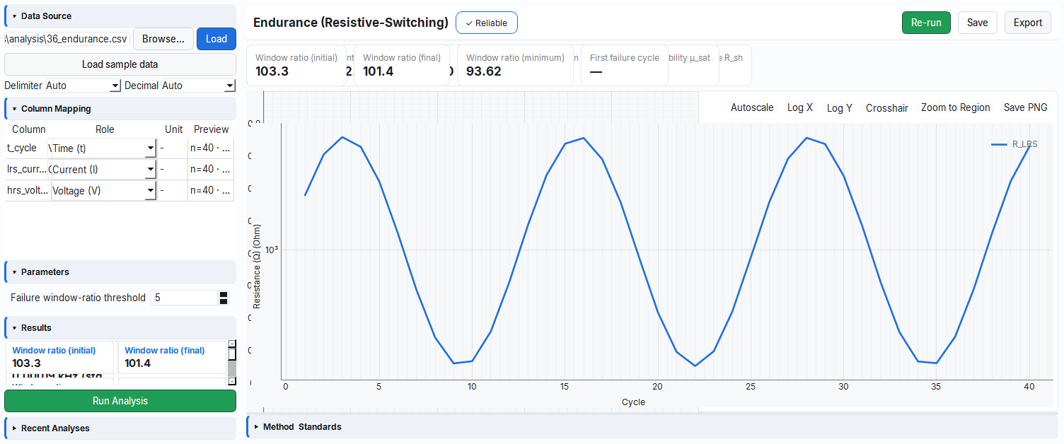
Resistive-switching memories (RRAM/memristor) store information by toggling between two states, "low resistance" and "high resistance." This test makes the device write-erase thousands of times and monitors how long the two states stay distinct from each other. It is like switching a light switch on and off thousands of times and counting when it starts to stick.
Physical background: A resistive-switching memory forms a conductive filament inside with a SET pulse and goes to low resistance (LRS), then breaks the filament with a RESET pulse and goes to high resistance (HRS); after each write, a small read resistance that does not disturb the state is measured. Over many cycles, when the filament fatigues, the two states approach each other (the R_HRS/R_LRS window closes) and an endurance failure occurs. On the semi-log plot, LRS and HRS draw two separate plateaus at first; the cycle where these plateaus begin to approach each other signals the end of life.
- Why it is done: To measure how many write-erase cycles the memory withstands and when it degrades.
- What it teaches / measures: R_LRS / R_HRS = the low/high resistance states; window ratio = R_HRS/R_LRS = the readability margin of the two states; first-failure cycle = the cycle where the window drops below the threshold (the endurance limit).
- Typical values and their interpretation: a window ≳10 is comfortably read (in mock LRS ~1.5 kΩ, HRS ~5 MΩ → a very wide window); when the window drops below failure_window_ratio (e.g., 5) it is counted as a "failure"; a good RRAM can withstand 10⁶–10⁹ cycles.
- Common mistakes / cautions: choosing the read voltage (read_voltage_v) too high and disturbing the state while reading it (read-disturb); setting the SET/RESET compliance wrong and over/under-forming the filament; overlooking that the window must be evaluated by the R_HRS/R_LRS ratio rather than absolute resistance.
- Where it is used: new memory/synaptic device research and endurance qualification.
Module: measure.endurance · Navigation: Endurance (SET/RESET Cycling)
Purpose: An endurance test for resistive-switching memory (RRAM / memristor / synaptic transistor). In each cycle a SET and a RESET write pulse are applied to the drain; after each write, the resistance is read with a small read pulse that does not disturb the state. The gate is held fixed (gate-tunable: a different V_G shifts the switching window).
What it measures: Two resistance readings per cycle — after SET → R_LRS (low resistance state), after RESET → R_HRS (high resistance state). R = |V/I|.
| Parameter | Unit | Description | Default |
|---|---|---|---|
n_cycles | — | Total number of cycles | 100 |
set_voltage_v / reset_voltage_v | V | SET / RESET write pulses | 2.0 / -2.0 |
write_pulse_width_s | s | Write pulse duration | 0.2 |
read_voltage_v | V | Read pulse (small voltage that does not disturb the state) | 0.2 |
read_pulse_width_s | s | Read settling/pulse duration | 0.01 |
read_samples | — | Samples per read (average) | 5 |
gate_voltage_v | V | Fixed gate bias (gate-tunable) | 0.0 |
inter_pulse_delay_s | s | Additional delay between pulses | 0.0 |
failure_window_ratio | — | "Failure" when HRS/LRS drops below this ratio | 5.0 |
current_compliance | A | Drain/gate current limit | 1e-2 |
Computed metrics:
| Metric | Formula | Unit |
|---|---|---|
| R_LRS / R_HRS (first & last) | After SET/RESET R = |V/I| | Ω |
| Window ratio | window = R_HRS/R_LRS (first/last/minimum) | — |
| First-failure cycle | The first cycle where the window drops below failure_window_ratio | — |
| Completed cycles | Number of cycles collected | — |
Plot: R-cycle (semi-log; R_LRS / R_HRS against cycle).
E. Temperature and Mapping Modules
E.1 Temperature-Dependent I-V (T-IV)
It repeats the same I-V measurement at a series of different temperatures. Since the behavior of semiconductors changes with temperature, by tracking this change we can extract the physical mechanisms inside the device (barriers, activation energy). It is like trying a recipe at different oven temperatures and extracting the rule behind the baking.
Physical background: The thermionic emission current depends very strongly on temperature (I0 ∝ T²·exp(−qΦ_B/kT)). Taking I-V at several temperatures and plotting the Richardson plot (ln(I0/T²) against 1/T) gives the barrier height (Φ_B) from the slope and the effective Richardson constant (A**) from the intercept. The activation energy (E_a) is extracted from the ln(I0)–1/T slope. The regular opening of the color-coded I-V family with temperature (more current at higher T) and the Richardson plot being a straight line confirm that the conduction mechanism is genuinely thermionic emission.
- Why it is done: To extract fundamental physical quantities from the temperature dependence of conduction and to verify the conduction mechanism.
- What it teaches / measures: Φ_B = the temperature-independent "true" barrier height; A** = the effective Richardson constant (a material/interface fingerprint); E_a = activation energy; dn/dT = the temperature trend of the ideality (a sign of barrier inhomogeneity).
- Typical values and their interpretation: for Si Schottky Φ_B ~0.6–0.85 eV; the theoretical A** for Si is ~110–120 A/cm²K² (deviation points to inhomogeneity); n increasing as the temperature drops (dn/dT<0) is the classic sign of barrier inhomogeneity.
- Common mistakes / cautions: choosing too narrow a T range and weakening the Richardson fit; measuring before the setpoint is truly reached (insufficient t_settle_time_s / t_tolerance_k); leaving the same fit range at every T and entering the bent region; forgetting that A** and Φ_B are sensitive to the active area.
- Where it is used: conduction mechanism research and the device's reliability over a temperature range.
Module: measure.tiv · Navigation: Temperature-Dependent I-V
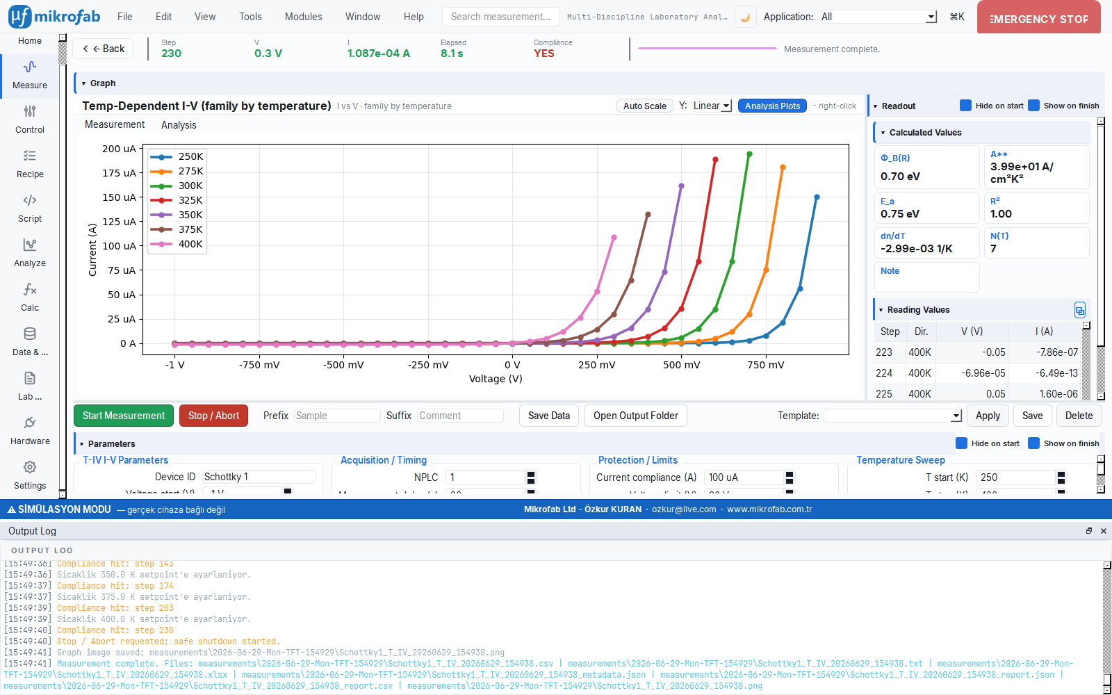
Purpose: Over a series of temperature setpoints, it takes a complete (Schottky) I-V sweep at each temperature; from each curve it extracts n(T), I0(T), Φ_B(T), R_s(T) and, from the Richardson plot, finds the aggregate barrier height and the effective Richardson constant (A**). Temperature control is done through an abstract TemperatureController (Phase 1: Simulated/Mock; Lakeshore 331/335/340 are supported).
What it measures: A temperature color-coded I-V family; temperature-resolved parameters.
| Parameter | Unit | Description | Default |
|---|---|---|---|
voltage_start / voltage_stop / voltage_step | V | The I-V sweep at each T | -1.0 / 1.0 / 0.05 |
current_compliance | A | Current limit | 1e-2 |
t_start_k / t_stop_k / t_step_k | K | Temperature sweep | 250 / 400 / 25 |
t_settle_time_s | s | Max stabilization after setpoint | 30.0 |
t_tolerance_k | K | Tolerance for reaching the setpoint | 2.0 |
t_controller_type | — | Simulated / Lakeshore 331/335/340 | Simulated |
t_controller_resource | — | VISA resource | GPIB0::2::INSTR |
A_richardson | A/cm²K² | Richardson constant | 110.0 |
device_area_um2 | µm² | Active area | 10000.0 |
Computed metrics:
| Metric | Formula | Unit |
|---|---|---|
| Φ_B (Richardson) | ln(I0/T²) = ln(A**·Area) − (qΦ_B/k)·(1/T) → Φ_B = −slope·k·1000/q | eV |
| A** (effective Richardson) | A** = exp(intercept)/Area | A/cm²K² |
| E_a (activation energy) | From the slope of ln(I0) vs 1000/T | eV |
| dn/dT | Linear slope of n(T) | 1/K |
| Temperature-resolved series | n(T), I0(T), Φ_B(T), R_s(T) | — |
Plot: I-V per T (temperature color-coded curve family).
I0(T) = A**·T²·Area·exp(−qΦ_B/kT), Φ_B = 0.72 eV, n(T) = 1.5 + 200/T; thus the Richardson analysis recovers Φ_B=0.72 and A**. The real waits are skipped.E.2 Device / Wafer Map
It repeats the same measurement at many positions on a wafer and plots the results as a colored map. This way you can see at a glance whether the production is of the same quality everywhere on the wafer. It is like taking soil samples from different corners of a field and producing a fertility map.
Physical background: At each position the selected base measurement is run and the distribution of the resulting parameter across the surface is plotted. The variation in the distribution reflects the non-uniformity of the production process (coating thickness, doping, annealing gradients); the heat map makes center-edge or systematic trends visible. Uniformity is quantified by std/mean (small = more uniform). This is not a device-physics measurement but the spatial statistics of many individual measurements.
- Why it is done: To evaluate how uniform the production is across the surface.
- What it teaches / measures: Parameter distribution (mean/std/min/max); uniformity = std/mean = a measure of uniformity; spatial gradient pattern (center-edge, etc.).
- Typical values and their interpretation: in a mature process a uniformity of a few % (std/mean ≪0.1) is considered good; a large std/mean or a strong edge gradient points to a process problem.
- Common mistakes / cautions: missing the true gradient with too sparse a grid; mistaking a single outlier (a poorly contacted position) for a process variation; wrong probe placement in the assisted mode; not ensuring that the base_measurement runs under the same conditions at every position.
- Where it is used: production/process quality control and process uniformity analysis.
Module: measure.device_map · Navigation: Device / Wafer Map
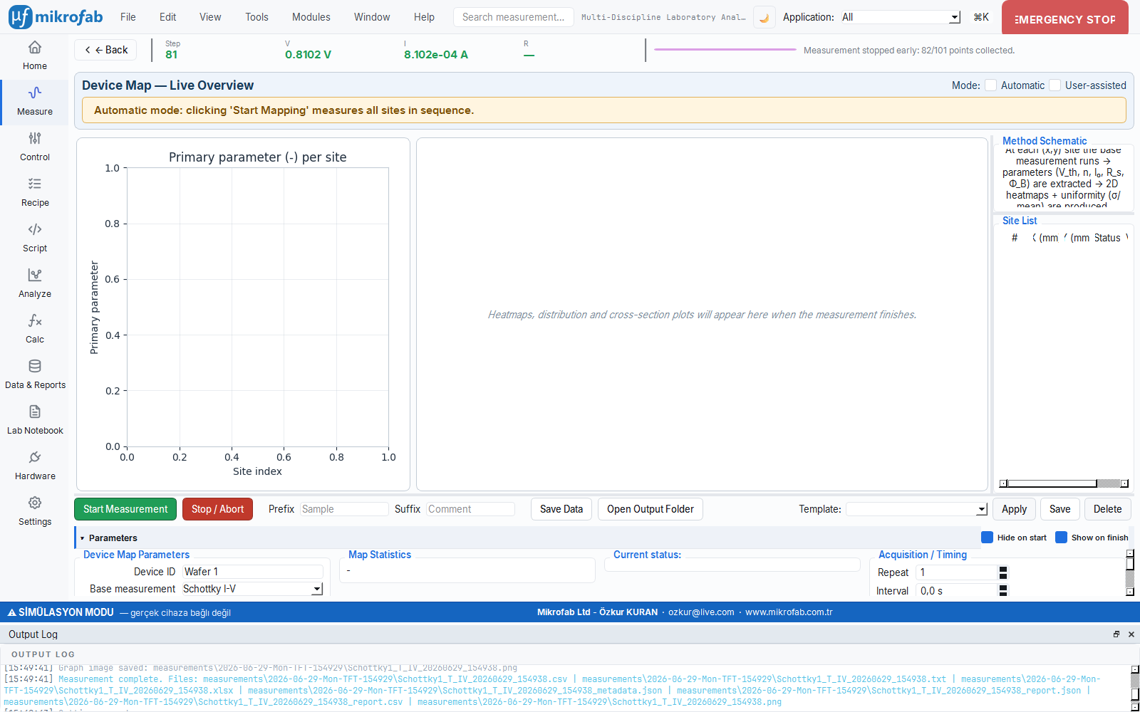
Purpose: Over a grid (x,y), it runs the selected base measurement at each position and extracts the selected parameters; it produces a 2D heat map and a uniformity statistic per parameter. It is used to evaluate spatial uniformity over a wafer/sample.
What it measures: At each (x,y) position, the parameters derived from the base_measurement (e.g., V_th, n, I0, R_s, Φ_B).
| Parameter | Unit | Description | Default |
|---|---|---|---|
base_measurement | — | The base measurement run per position | Schottky I-V |
x_positions_mm / y_positions_mm | mm (list) | Grid positions | [0,5,10,15,20] |
map_params | — (list) | Parameters to be mapped | [V_th, n, I_0, R_s, Phi_B] |
inter_device_delay_s | s | Delay between positions in automatic mode | 2.0 |
assisted | — | Assisted mode (confirmation at each position) | False |
Two operating modes: Automatic (sequential, with inter_device_delay) and Assisted (before each position the user positions the probe/stage and says "Measure this position"; the GUI continues via a gate/Event).
Computed metrics: Per parameter, mean, std, min, max and uniformity = std/mean. The output returns a grids[param][iy][ix] grid and a statistics block per parameter.
Plot: Map grid (2D heat map).
param(x,y) = nominal·(1 + 0.05·G(x,y) + small noise), where G(x,y) is a normalized Gaussian profile peaking at the grid center (realistic center-edge uniformity). On real hardware the base_measurement is run at each position.Summary: Module → Plot → Metric Mapping
Module (id) | Navigation | Plot | Main metrics |
|---|---|---|---|
measure.iv | Output — Vds–Vgs | Id-Vd | R_on, r_o, λ, µ_sat |
measure.transfer | Transfer | Id-Vg lin/log, gm-Vg | V_th, µFE, SS, I_on/I_off, ΔV_th |
measure.pulsed_iv | Pulsed I-V | Id-t | (self-heating transient) |
measure.qpulsed | Q-Pulsed I-V | Id-t | ΔV_th, N_t |
measure.hw_sweep | Hardware Vds–Vgs | Id-Vd | (fast list sweep) |
measure.hw_tft_sweep | Hardware TFT I-V | Id-Vg | (fast transfer) |
measure.diode | Diode I-V | I-V lin/log | n, I0, V_on, R_s |
measure.schottky | Schottky I-V | I-V log | Φ_B, n, R_s, J0 |
measure.rev_recovery | Reverse Recovery | I-t | t_rr, I_rr, Q_rr, τ |
measure.four_point | Four-Point | R readings | R_s, ρ, σ |
measure.vdp | Van der Pauw / Hall | VDP map | R_s, µ, n, n_s |
measure.kelvin | Kelvin 4-Wire | R-I | R_4wire, R_contact |
measure.probe_iv | Probe Station I-V | I-V | R, G |
measure.bias_stress | Bias Stress / Transient | Id-t | (drift) |
measure.bias_stress_enh | Bias Stress (Enhanced) | Id-t, Vth-t | ΔV_th, p, MTTF |
measure.endurance | Endurance | R-cycle | R_LRS, R_HRS, window, failure cycle |
measure.tiv | Temperature-Dependent I-V | I-V per T | Φ_B, A**, E_a |
measure.device_map | Device / Wafer Map | Map grid | regional statistics |