One software, two worlds
Mikrofab Suite brings the quality engineer on the production line and the PhD student in the research group together in the same interface. The same measurement core, the same traceable report, the same simulation mode — only the data source and the goal change.
R&D, manufacturing and quality control
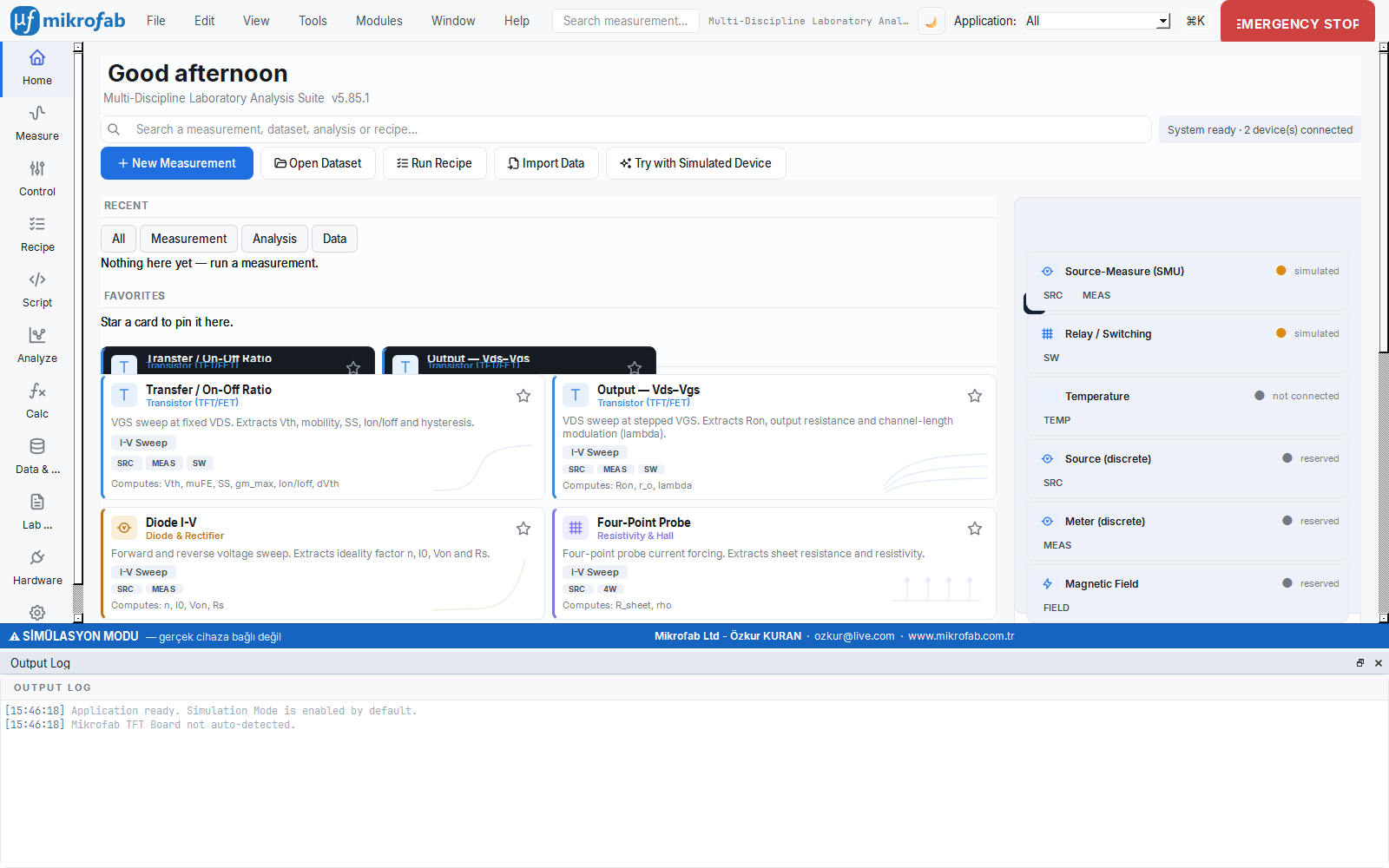
- R&D teams: characterize new materials and device architectures quickly; use 37 measurement modes and 37 analysis modules in a single package.
- Manufacturing and fab: scan many devices across a wafer with a single launch using a relay/switch matrix.
- Quality control: document batch-to-batch consistency with uniformity maps and traceable reports.
- Wafer mapping: view the parameter distribution across the grid as a 2D heat map.
- Overnight automation: set up unattended, all-night test campaigns with recipes and headless mode.
Research, teaching and the laboratory
- Research groups: combine semiconductor, photovoltaic, LCR/impedance and resonant spectroscopy in a single environment.
- University laboratories: bring your existing multi-vendor instrument park together under one common interface.
- Teaching and coursework: thanks to simulation (mock) mode, every student can work without hardware on their own computer.
- Multidisciplinary projects: with the Lab Notebook (ELN), keep the sample lifecycle in one place — from process steps to electrical results.
The work you face every day
Not abstract features, but concrete scenarios. The six workflows below are what professional and academic users do most with Mikrofab Suite — each shown together with the concrete benefit it delivers.
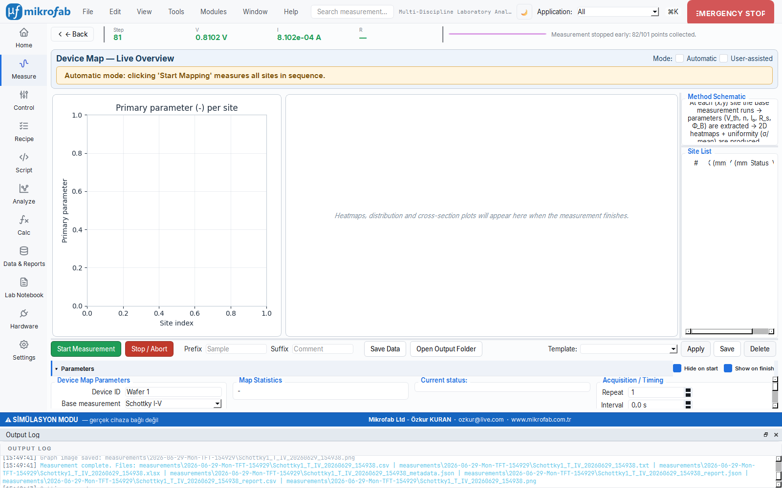
Wafer and device mapping
Automatically run the same base measurement at every position on a grid (x, y); for each parameter you get a 2D heat map and the uniformity = std/mean statistic. See center-edge variation, dead zones and process drift at a glance.
Overnight batch tests
Run dozens of measurements unattended with recipes and headless mode; repeat through the night with --repeat / --interval. Because every point is written to disk instantly, your data is safe even if power is lost, and the results are ready in the morning.
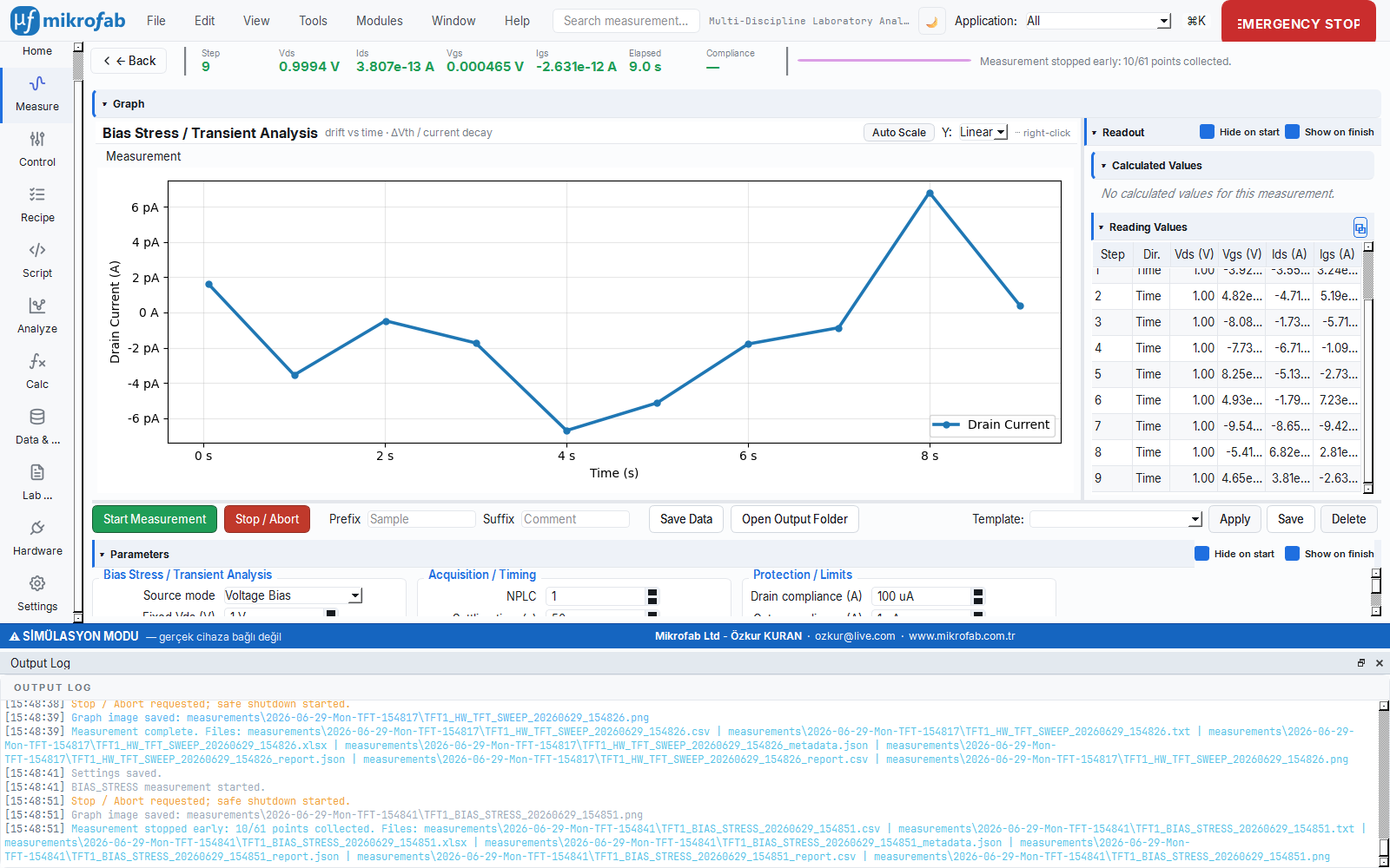
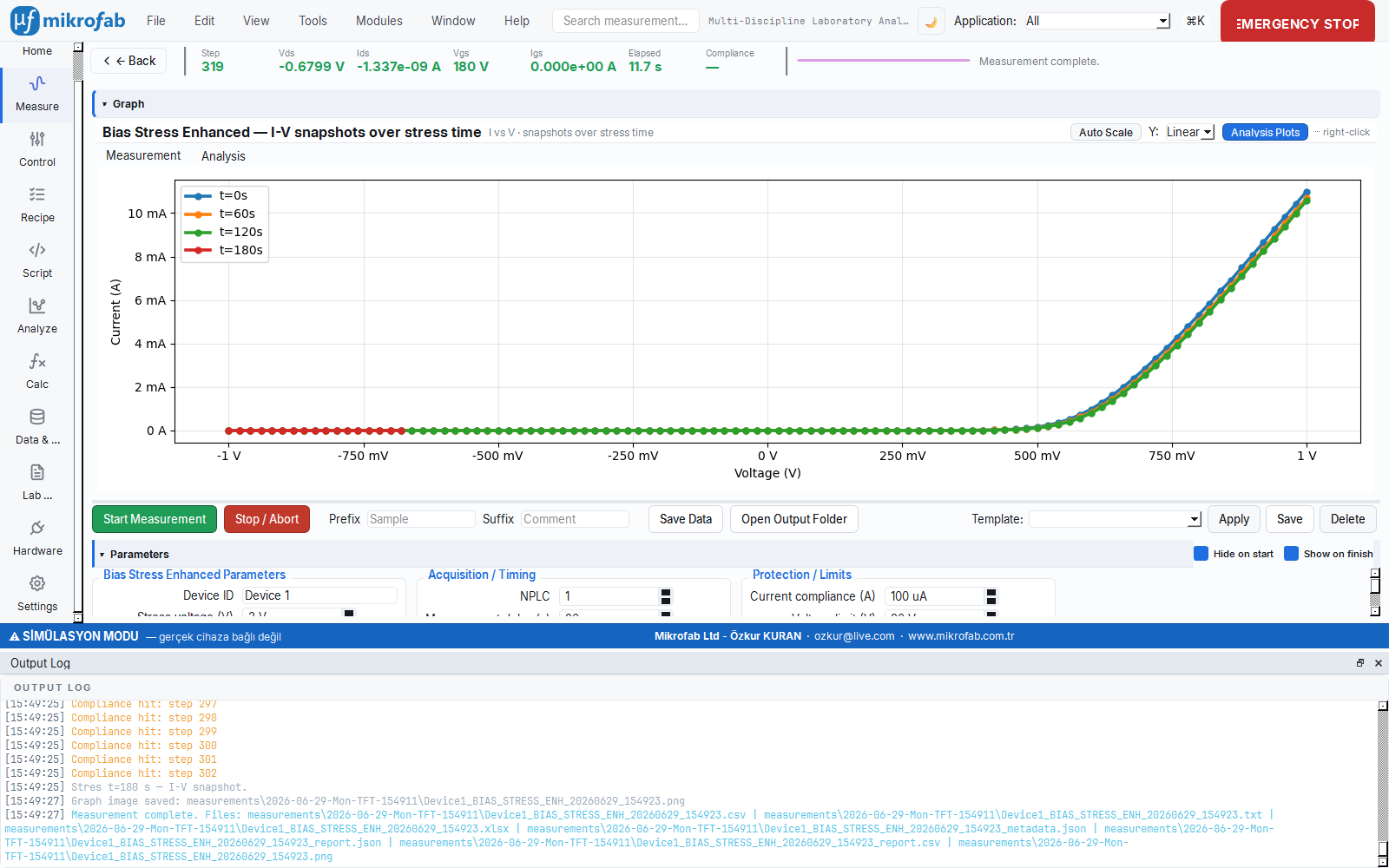
Bias stress and endurance
Track the drift of drain current and threshold voltage (ΔV_th) under constant bias; extrapolate MTTF with a power-law fit. For RRAM/memristors, measure the HRS/LRS window and the first-failure cycle across SET/RESET cycling.
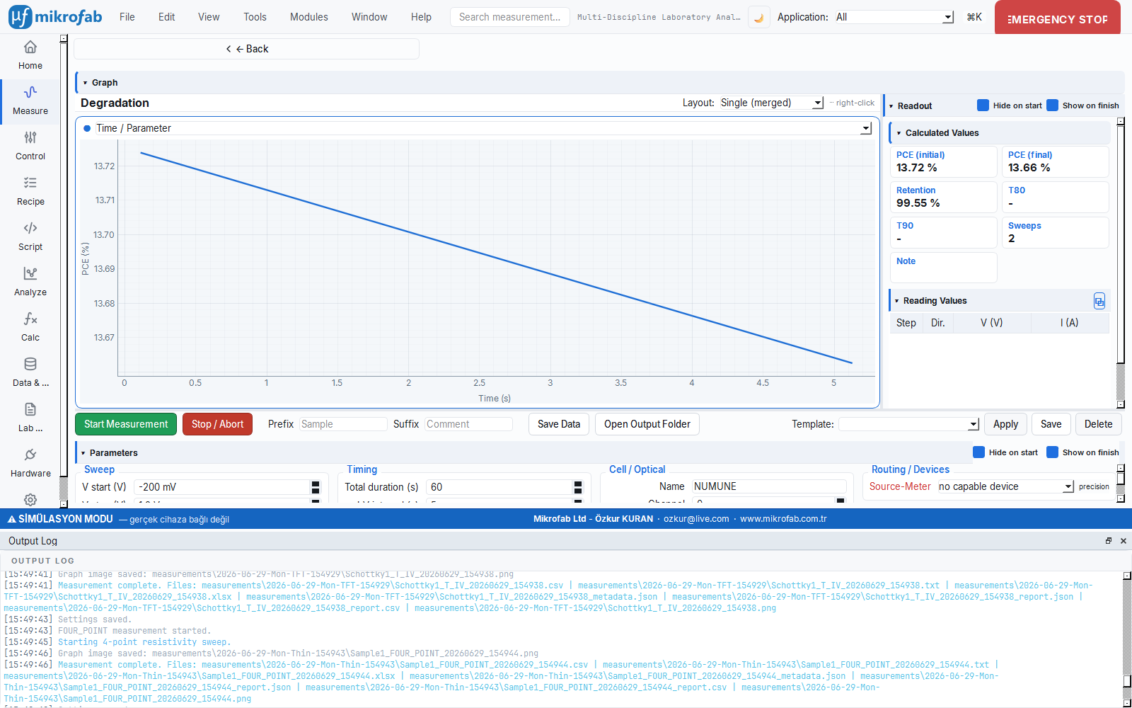
Solar cell stability
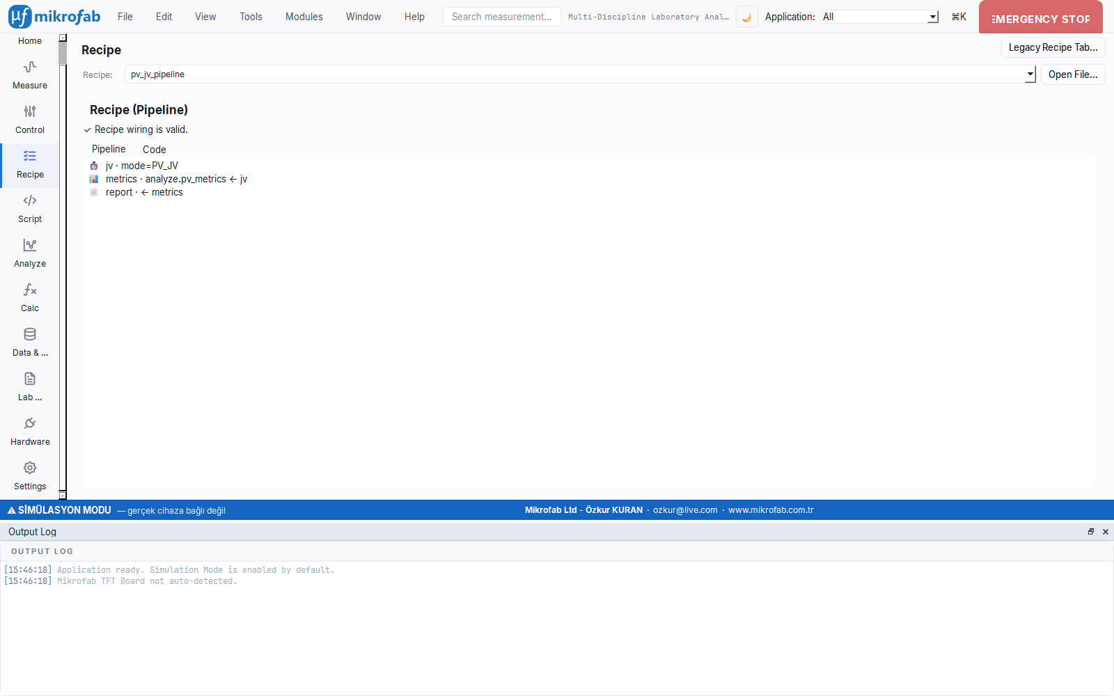
Record how PCE, FF and Voc change over time under light and thermal aging; quantify lifetime and degradation rate with stability (degradation) curves. A complete PV workflow with J-V, MPPT and Suns-Voc.
Teaching laboratory (simulation)
The built-in simulation (mock) mode generates physically consistent synthetic data. Students learn all measurement modes and the analysis workflow on their own computer without hardware; ideal for lectures, demos and validation.
Multi-vendor instrument park
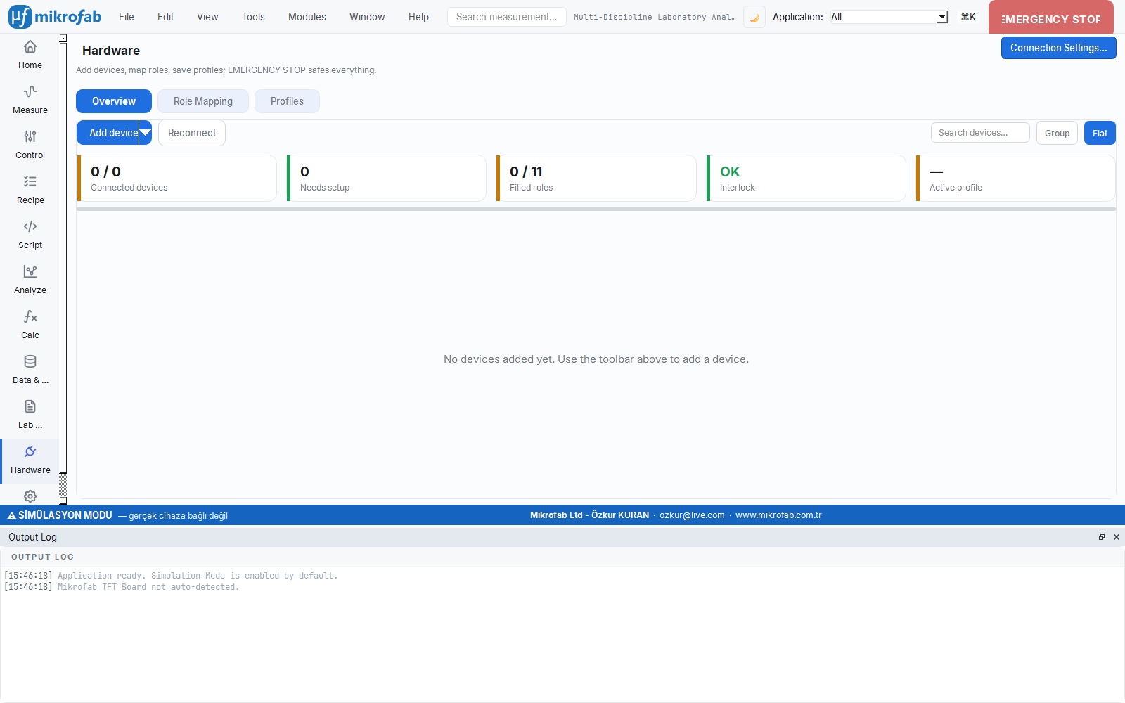
Drive Keithley, Keysight and R&S SMUs from the same interface; with a relay/switch matrix, scan many devices on a wafer in a single launch. Connect your existing hardware to a common workflow without replacing it.
Two flagship workflows
Examine the two scenarios professional users turn to most often, together with their screens.
One launch, results ready by morning
The classic recipe automates the standard flow of TFT stability: a pre-stress transfer curve, a period of bias stress, a post-stress transfer — and you have the threshold shift (ΔV_th). With headless mode, you repeat this all night, unattended.
- The Transfer-Before → Bias Stress → Transfer-After chain is repeated in sequence for each selected TFT.
- Repeated runs with
--repeat N --interval S; for example, an eight-hour stress (bias_duration_s = 28800). - Crash-resilient
*_partial.csv: even if power is lost, the data up to that moment is preserved. - Unique, timestamped output folders — no conflict copies are created in synced folders such as OneDrive.
- Start/monitor/stop remotely with the local REST API;
Ctrl+Calways brings the system to a safe state.
See uniformity across the wafer
The Device/Wafer Map module runs the base measurement you choose at every position on a grid and pours the results into a spatial heat map. Perfectly suited to documenting uniformity in manufacturing and finding the best region in R&D.
- Automatic or user-assisted mode: position the probe at each location and confirm, or run them all in sequence.
mean,std,min,maxand uniformity = std/mean per parameter.- A separate 2D heat map for each mapped quantity (V_th, n, I_0, R_s, Φ_B …).
- With the relay matrix, scan many devices on a single wafer without operator intervention.
Scenarios on screen
Real interface views for the reliability, photovoltaic stability, teaching and multi-vendor integration scenarios.
Let's build the solution that fits your workflow, together
Whether you document uniformity on the production line or characterize a new material in the lab — try Mikrofab Suite with your own scenario. Contact us about the trial version and licensing model; let's schedule a live demo for you.