Calculation Workshop and Physics Reference
This section gathers, in one place, the Calculation (Calc) workspace of the Mikrofab semiconductor/TFT/PV measurement software together with the central physics/mathematics reference behind every quantity the application derives. The Calc workspace is the workshop where you perform laboratory calculations without touching any instrument — that is, by entering values manually: four-point-probe sheet resistance, van der Pauw + Hall, solar-cell fill factor, photodetector responsivity, and a free-form formula notebook. With a transparency-first philosophy, every calculator clearly shows the input → formula → output → unit → underlying standard.

This section combines two things: a "workshop" in which, without ever touching an instrument, you enter your measured numbers and have laboratory quantities computed (resistance, mobility, efficiency, responsivity...), and a reference shelf collecting the formulas behind all of those calculations. Think of it as a kitchen scale + a recipe book: you place the number and read the result, and whenever you are curious you find the full recipe (formula) in the same place.
- Why it is done: to learn what your raw measured numbers (voltage, current, frequency...) mean and which material property they correspond to.
- What it teaches / measures: it shows each calculation transparently through an "input → formula → output → unit → standard" chain; you can see where the result comes from.
- Where it is used: when preparing a course/experiment report, when manually verifying a measurement result, and when you want to recall the physics of a quantity.
1. Structure of the Calc workspace
The Calc workspace consists of two usage modes:
| Mode | i18n / title | What it does |
|---|---|---|
| Quick Calc (secure formula) | shell.calc.scratch | Free-form formula notebook + numerical differentiation/integration (scientific calculator) |
| Method Library (compute engines) | shell.calc.methods | Ready-made, validated calculator modules (the 8 engines below) |
At the top, a search box (shell.calc.search_placeholder — "Search calculations…") filters the modules by title/label; if there is no match, "No matching calculator." is shown.
Each calculator module is kept in the registry under the key calc:<id> and is loaded from the following eight executable ComputeSpec files (app/calc_kit/compute_specs/):
| Registry key | Title | Category | Schematic (diagram) |
|---|---|---|---|
calc:four_point_probe | Four-Point Probe (collinear) | Resistance Measurement | four_point_probe |
calc:fpp_correction_circular | 4PP Correction — Circular Substrate | Resistance Measurement | fpp_circular |
calc:fpp_correction_rectangular | 4PP Correction — Rectangular Substrate | Resistance Measurement | fpp_rectangular |
calc:fpp_correction_thick | 4PP Correction — Thick Substrate | Resistance Measurement | fpp_thick |
calc:sheet_resistance_vdp | Sheet Resistance (van der Pauw) | Resistance Measurement | van_der_pauw |
calc:van_der_pauw_hall | Van der Pauw + Hall Worksheet | Resistance Measurement | van_der_pauw_hall |
calc:pv_metrics_manual | Solar Cell — Fill Factor & Efficiency | Solar Cell | solar_jv |
calc:responsivity_from_power | Responsivity (Photocurrent / Power) | Photodetector | responsivity |
Each module panel consists of three layers: at the top a theme-aware schematic drawing + legend, in the middle live input fields (numeric spin boxes), and at the bottom output cards. Every time you change an input, all outputs are recomputed instantly.
eval/exec, through a hand-written AST allow-list (app/calc_kit/formula.py). Attribute access, imports, lambdas, and slicing/subscripting are forbidden; only allowed math functions (sin, cos, tan, log, ln, sqrt, cbrt, exp, abs, factorial, gamma, erf, atan2, hypot…) and constants (pi, e, tau) may be called. An invalid grammar or a runtime math error is not silently swallowed — it raises a loud error (Calc is "noisy").2. Quick Calc (free-form formula notebook + numerical calculus)
It is a smart calculator in which you write your own formula and instantly get its result; it also finds the slope of a function (derivative) or the area beneath it (integral) numerically. Like a live Excel cell whose variables you can fill in: you write the formula once, and as you change the numbers the result updates immediately.
- Why it is done: to quickly perform a small, custom calculation for which there is no ready-made module.
- What it teaches / measures: the result of an expression and, if desired, the rate of change at a point (derivative) or the cumulative total (integral).
- Where it is used: quick sanity-check calculations, unit conversions, and the "let me just compute this" moments during homework/experiments.
Quick Calc is a small scientific calculator in which you write an arithmetic formula with variables. The moment you type the formula, the widget validates it live, opens an automatic numeric input field for each free variable, and computes the result live.
Step-by-step usage
- Type an expression into the Formula field (e.g.
V * V / R). - An input box appears automatically for each variable (V, R, …); enter the values.
- The result appears instantly as
Result: {value} {unit}. The unit field is only a label (e.g.W); it does not enter the calculation. - If desired, from the CALCULUS (NUMERICAL) section below, select a variable and take its derivative/integral.
| Field | Unit | Description | Default |
|---|---|---|---|
| Formula | — | Arithmetic expression (allowed functions + constants) | empty |
| (automatic variables) | — | A numeric field for each free name in the formula | 0.0 |
| Unit | — | Free-text label shown next to the result | empty |
| Derivative f′ at point | — | Numerical derivative of the var variable at the given point | 1.0 |
| Integral ∫ lower / upper | — | Lower and upper limits of the definite integral | 0.0 / 1.0 |
Numerical methods (pure Python, no numpy/scipy/sympy):
- Derivative: 5-point central stencil, O(h⁴) accuracy:
Formula f′(x) ≈ [−f(x+2h) + 8f(x+h) − 8f(x−h) + f(x−2h)] / (12h)
- Integral: composite Simpson's rule (1000 subintervals), ~1e-9 accuracy for smooth functions. The limits may be given in reverse order; the sign is corrected automatically.
All other variables are held fixed at their values in the context; the value of the calculus variable is varied by the sampling point/integration limit.
log(x) is the natural logarithm; log(x, base) gives the logarithm to that base. By calculator convention, ln(x) is also a shortcut for the natural logarithm. factorial works only for non-negative integers; for a non-integer argument use gamma(x+1).shell.calc.calculus.hint). A sampling point at the domain boundary of functions like log/sqrt (e.g. the square root of a negative number) blows up the calculation and a "—" error message appears.3. Calculator modules (Method Library)
Below, for each of the eight executable modules, the input → formula → output → unit → standard is given. All resistance modules use laboratory units: voltage in mV, current in mA, length in mm/µm. Since V/I is a ratio, the mA/mV scaling cancels and the result comes out directly in the desired unit.
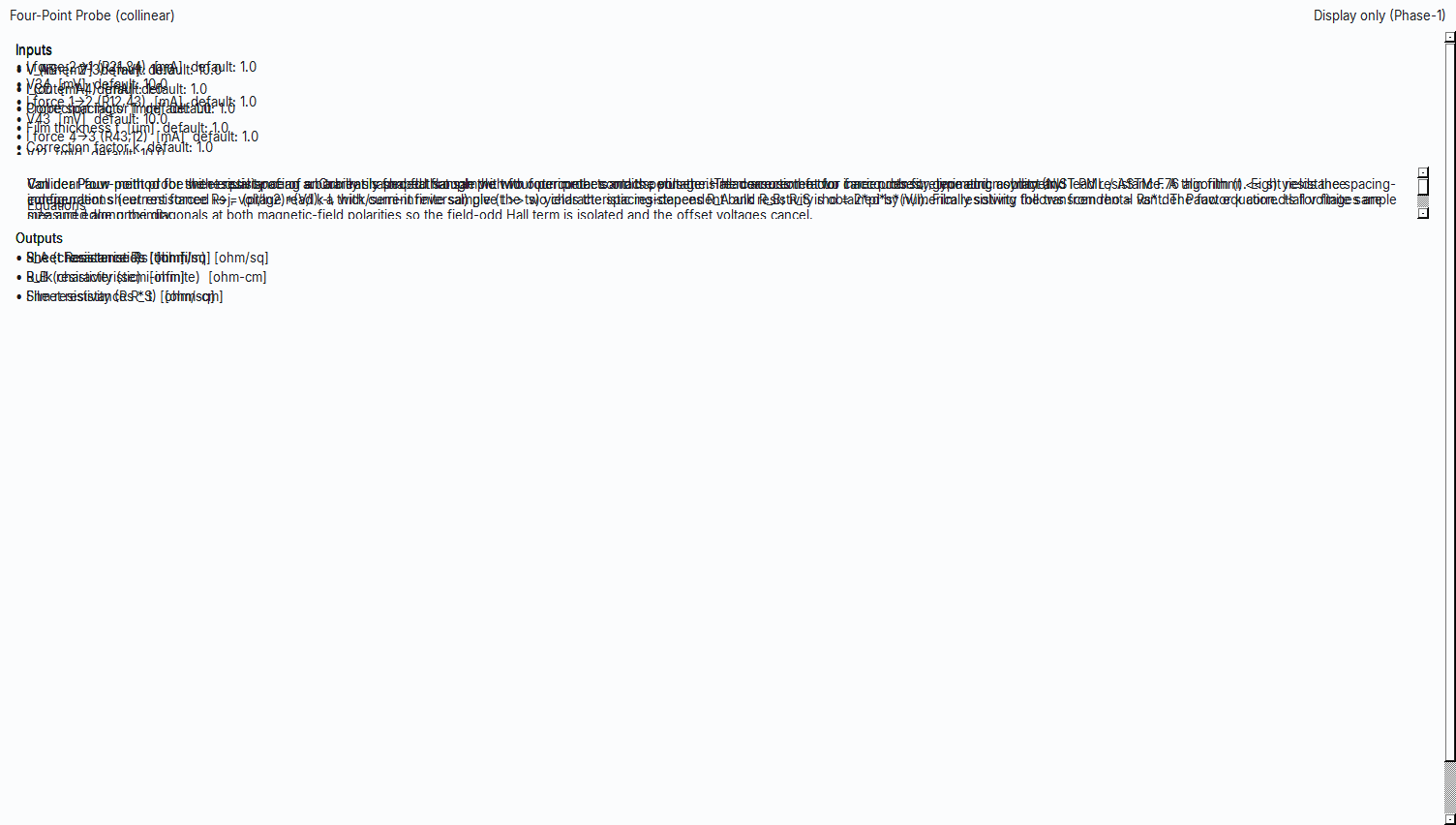
3.1 Four-Point Probe (collinear) — calc:four_point_probe
It lets you measure how easily a thin film or sheet conducts electricity by touching four needles to its surface. Current is forced through the outer two needles, and voltage is read from the inner two; because the voltmeter draws almost no current, the resistance of the cables and contact points does not contaminate the result. Like measuring how "smooth" (conductive) a road is without counting the entry/exit toll booths.
Physical background: The current forced through the outer probes spreads into the film and, between the inner probes, produces an IR voltage drop arising solely from the material's resistance. Because the current spreads two-dimensionally (laterally) in a thin sheet, the geometric constant π/ln2 ≈ 4.5324 emerges and the result becomes independent of probe spacing — the current-density profile scales together with the spacing. When the sample becomes thick relative to the probe spacing, current spreads three-dimensionally and the formula changes (volume resistivity becomes spacing-dependent).
- Why it is done: to determine the conductivity quality of a coating/film, free of contact resistance.
- What it teaches / measures: sheet resistance Rs (Ω/sq) = the resistance across a unit square, a thickness-independent film "fingerprint"; resistivity ρ (Ω·cm) = the intrinsic conduction property of the material, free of thickness (ρ = Rs·t); correction factor k = the coefficient that compensates for edge effects in a finite sample.
- Typical values and interpretation: metal films <1 Ω/sq (even mΩ/sq); transparent conductive ITO ~10–100 Ω/sq (good for displays/touch); doped semiconductor films ~10²–10⁴ Ω/sq; a very high Rs is a sign of poor doping/conduction or a very thin/discontinuous film.
- Common mistakes / cautions: applying the thin-film formula to a thick sample (or vice versa); leaving k=1 for a finite sample and neglecting the edge effect; heating the sample with excessive current; unequal probe spacing or unstable contact pressure.
- Where it is used: process control in semiconductor manufacturing, quality inspection of transparent conductive (ITO) and metal films.
An equally spaced (s), collinear four-point probe. Current is forced through the outer probes (1 and 4) and voltage is read from the inner probes (2 and 3); this eliminates contact and cable resistance.
| Parameter | Unit | Description | Default |
|---|---|---|---|
| V (inner 2-3) | mV | Voltage between the inner probes | 10.0 |
| I (outer 1-4) | mA | Current forced through the outer probes | 1.0 |
| Probe spacing s | mm | Equal probe spacing (converted to cm by ×0.1) | 1.0 |
| Film thickness t | µm | Film thickness (converted to cm by ×1e-4) | 1.0 |
| Correction factor k | — | Geometric/edge correction (1 for an ideal large sample) | 1.0 |
Formulas and outputs
| Output | Formula | Unit | Validity |
|---|---|---|---|
| Sheet resistance Rs (thin film) | Rs = (π/ln2)·(V/I)·k | Ω/sq | Thin film, t ≪ s; independent of s |
| Volume resistivity (semi-infinite) | ρ = 2π·s·(V/I) | Ω·cm | t ≫ s; proportional to s, k not applied |
| Film resistivity | ρ_film = Rs·t | Ω·cm | Film of known thickness |
π/ln2 ≈ 4.5324 is a geometric constant. There are two limiting cases: a thin film gives a spacing-independent sheet resistance; a thick/semi-infinite sample gives a spacing-dependent volume resistivity. The correction factor k is applied only to the thin-film sheet resistance, not to the semi-infinite volume resistivity (a different geometric assumption).
Standard: ASTM F84 · Smits (1958).
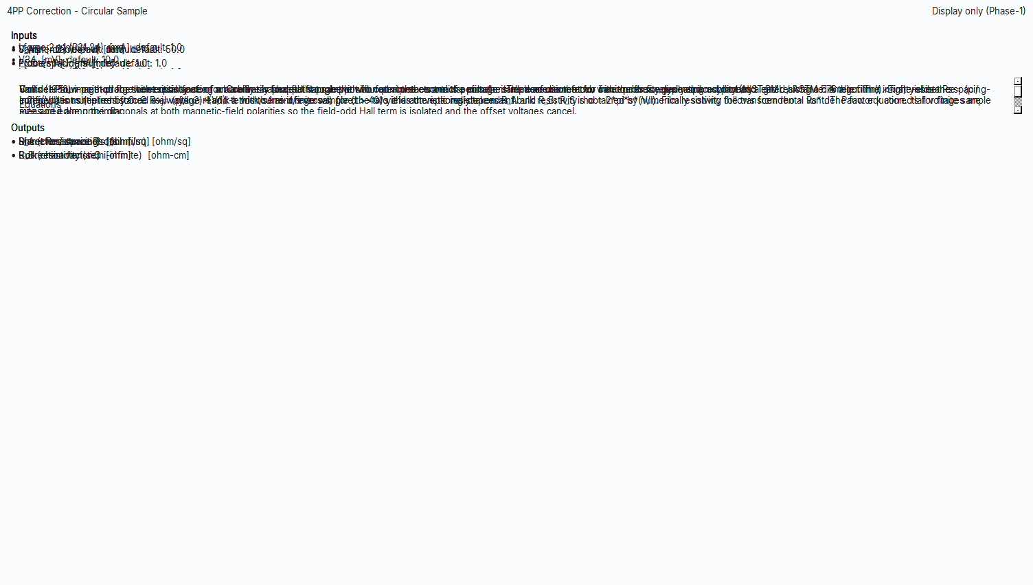
3.2 4PP Correction — Circular Substrate — calc:fpp_correction_circular
The four-point-probe formula assumes an "infinitely large" sample; a real round wafer is finite, and its edges squeeze the current. This module looks at the ratio of the wafer diameter to the probe spacing and gives a coefficient (C) that corrects the result. Like the edges of a small field restricting the water when you irrigate with a hose; the correction adds back this edge effect.
Physical background: In the ideal formula the current spreads freely sideways; in a finite wafer the insulating edge pushes the current back, which raises the voltage at the inner probes and makes the uncorrected Rs appear larger than it is. Smits's closed-form C factor removes exactly this excess; as the d/s ratio grows, the edge moves farther away and C → 1 (the correction becomes unnecessary).
- Why it is done: to remove the edge error that arises in a finite, circular sample.
- What it teaches / measures: the d/s ratio = the ratio of the wafer diameter to the probe spacing (how far the edge is); the correction factor C (≤ 1) = the coefficient to multiply the raw Rs by, to be entered into the
kfield of the Four-Point Probe calculation. - Typical values and interpretation: for d/s ≥ 40, C ≈ 1 (the correction is negligible); as d/s decreases, C drops below 1 (the edge effect grows). The farther C is from 1, the more important the edge correction is.
- Common mistakes / cautions: placing the probe near the edge of the wafer rather than at its center (the formula assumes the center); forgetting that in the region d/s < √3 (~1.732) the formula is mathematically undefined — in that case the module raises a loud error.
- Where it is used: sheet-resistance measurements made at the center of standard round semiconductor wafers.
The Smits (1958) closed-form geometric correction factor C for a collinear probe aligned along a diameter at the center of a circular wafer.
| Parameter | Unit | Description | Default |
|---|---|---|---|
| Sample diameter d | mm | Wafer diameter | 50.0 |
| Probe spacing s | mm | Equal probe spacing | 1.0 |
| Output | Formula | Unit |
|---|---|---|
| d/s | d/s | — |
| Correction factor C | C = ln2 / (ln2 + ln(((d/s)²+3)/((d/s)²−3))) | — |
C ≤ 1 and approaches 1 as d/s grows (the edge effect vanishes). Mathematically it is defined only for d/s > √3 (~1.732); below that the closed form is undefined and the sandbox raises a loud error. Physically it is reliable for d/s ≥ 3; for d > 40·s, C ≈ 1 is taken. The corrected sheet resistance is Rs_corrected = C·(π/ln2)·(V/I).
Standard: Sze (Physics of Semiconductor Devices) · GUM.
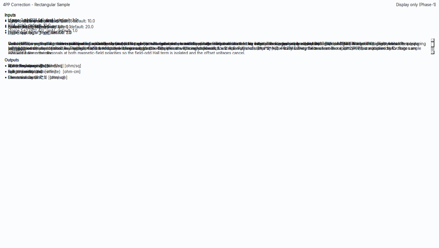
3.3 4PP Correction — Rectangular Substrate — calc:fpp_correction_rectangular
This is the version of the same edge-effect correction for rectangular (square/strip) samples. Since there is no closed-form formula, a value is read from a published table (Topsøe 1966) based on the width/length and probe-spacing ratios. Like looking up two measurements in a ready-made conversion table and reading the value in between.
Physical background: In a rectangular sample, two different edges (the short edge w and the long edge l) restrict the current spread to different degrees; therefore the correction depends not on a single ratio but on both the w/s and l/w ratios, and it has no analytic closed form. The software performs bilinear interpolation from the table based on the two ratios; values that fall outside the table are clamped to the nearest edge (no fabricated extrapolation).
- Why it is done: to correct the deviation caused by the edges in rectangularly cut samples.
- What it teaches / measures: w/s = the ratio of the short edge to the probe spacing; l/w = the length/width aspect ratio of the sample; the correction factor C = the coefficient read from these two ratios, to be entered into the
kfield. - Typical values and interpretation: the table is defined for w/s ∈ [1, 40] and l/w ∈ [1, 4]; the factor is reliable when w/s ≥ 3. Example: w=10, l=20, s=2 → w/s=5, l/w=2 → C=0.7887 (i.e. the raw Rs is corrected by more than 20%).
- Common mistakes / cautions: confusing width (w) and length (l) and entering l/w < 1 is a common error — the long edge must always be l; otherwise the module does not clamp but raises a loud error.
- Where it is used: square/strip-cut test coupons, coated samples on glass.
The Topsøe (1966) correction factor C for a probe placed at the center of a rectangular sample, parallel to the long edge. There is no closed form; it is read from the table by bilinear interpolation and clamped at the table edges (no extrapolation).
| Parameter | Unit | Description | Default |
|---|---|---|---|
| Sample width w (short edge) | mm | Short edge | 10.0 |
| Sample length l (long edge) | mm | Long edge (l/w ≥ 1) | 20.0 |
| Probe spacing s | mm | Equal probe spacing | 2.0 |
| Output | Formula | Unit |
|---|---|---|
| w/s | w/s | — |
| l/w | l/w | — |
| Correction factor C | C = table(w/s, l/w) (Topsøe; bilinear) | — |
The table is defined for w/s ∈ [1, 40] and l/w ∈ [1, 4]; outside this range the nearest value is used. The factor is reliable for w/s ≥ 3. Example: w=10, l=20, s=2 → w/s=5, l/w=2 → C=0.7887.
Standard: Sze · GUM (Topsøe 1966 data).
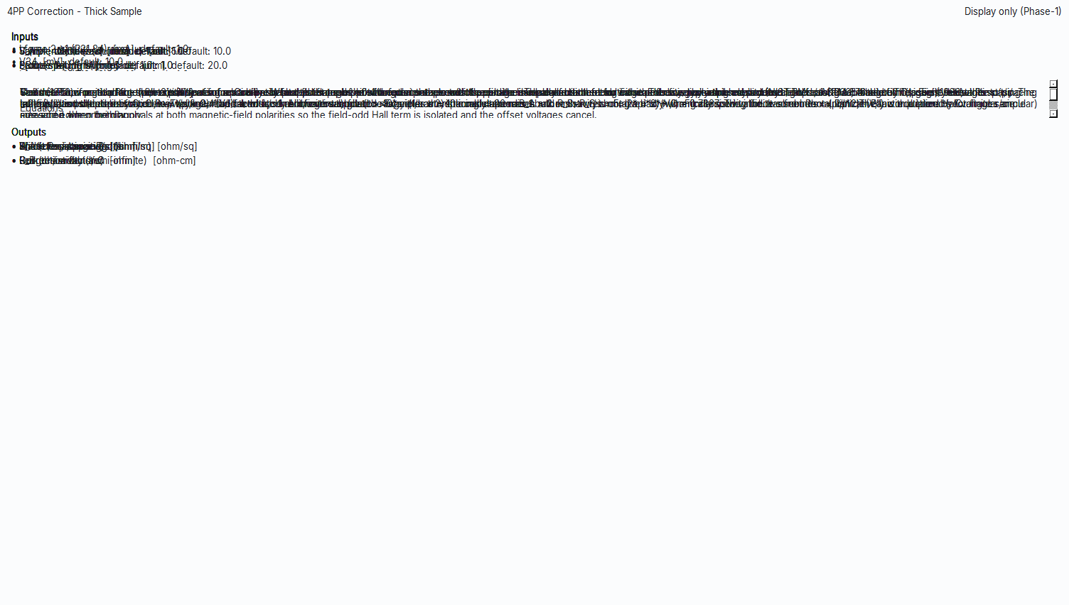
3.4 4PP Correction — Thick Substrate — calc:fpp_correction_thick
The thin-film formula assumes the sample is "paper-thin" relative to the probe spacing. As the sample gets thicker, the current no longer stays at the surface but spreads three-dimensionally; this module gives the coefficient that corrects for this, based on the thickness/spacing ratio. Like pouring water into a deep bucket instead of a shallow tray; the current now spreads downward as well.
Physical background: In the thin-film approximation, current flows only horizontally (2-D); as the sample thickens, the lower layers also participate in conduction, the effective cross-section increases, and the voltage at the inner probes drops. An uncorrected calculation therefore gives a resistance different from the true value; the Topsøe thickness factor C compensates for this three-dimensional spread based on the t/s ratio, and in the limit t/s → 0, C → 1.
- Why it is done: to remove the error in thick samples arising from the current spreading into the depth.
- What it teaches / measures: the t/s ratio = the ratio of thickness to probe spacing (how "thick" the sample is considered); the thickness correction factor C = the coefficient that combines multiplicatively with the lateral (circular/rectangular) correction.
- Typical values and interpretation: for t/s < 0.4, C ≈ 1 (thin-film limit, correction unnecessary); in the range 0.4 ≤ t/s ≤ 2 the table is valid and the correction becomes progressively more important; for t/s > 2 the closed-form correction is unreliable.
- Common mistakes / cautions: forcing the table in the region t/s > 2 — the module raises an error rather than returning a clamped, wrong value (a dedicated 3-D method is required); applying only the thickness C while forgetting the lateral correction (the two must be multiplied).
- Where it is used: resistivity measurements on thick sheet/block samples.
The thin-film formula assumes t ≪ s. When t/s > ~0.4, the current spreads three-dimensionally and the result must be scaled by the Topsøe (1966) thickness correction factor C. Linear interpolation is used.
| Parameter | Unit | Description | Default |
|---|---|---|---|
| Sample thickness t | mm | Thickness | 1.0 |
| Probe spacing s | mm | Equal probe spacing | 1.0 |
| Output | Formula | Unit |
|---|---|---|
| t/s | t/s | — |
| Correction factor C | C = table(t/s) (Topsøe; linear, 0.4 ≤ t/s ≤ 2) | — |
For t/s < 0.4, C ≈ 1 (thin-film limit). The table is valid only up to t/s = 2; above that the factor drops steeply and the module raises an error rather than returning a clamped, wrong value (a dedicated 3-D method is required). It combines multiplicatively with the lateral (circular/rectangular) correction.
Standard: Sze · GUM.
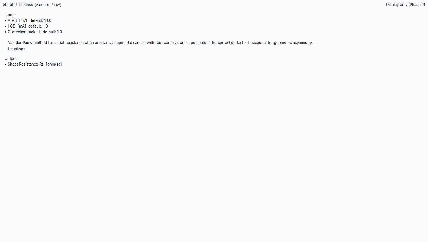
3.5 Sheet Resistance (van der Pauw) — calc:sheet_resistance_vdp
Instead of evenly aligned needles, this is the practical way to measure sheet resistance by placing four small contacts at the corners/edges of the sample. The sample's shape does not have to be regular; it only needs to be thin, hole-free, and singly connected (containing no slits or holes). Like measuring the depth of a pond not with a straight ruler but from four points along its edge and combining them with mathematics.
Physical background: The van der Pauw theorem establishes an exact relation, for four arbitrarily placed contacts on a thin, homogeneous sheet, between the current/voltage ratios and the sheet resistance; therefore the distance between contacts does not enter the formula. In this quick version a single symmetric configuration is used and the result is found directly via Rs = (π/ln2)·(V/I)·f (the full transcendental solution is in §3.6).
- Why it is done: to measure sheet resistance on irregularly shaped, small samples without needing a probe spacing.
- What it teaches / measures: sheet resistance Rs (Ω/sq) = the thickness-independent resistance fingerprint of the film; the f factor = a correction that compensates for sample/contact asymmetry (1 for perfect symmetry). The contact spacing does not enter the formula.
- Typical values and interpretation: the same orders of magnitude as 4PP apply (ITO ~10–100 Ω/sq, doped films 10²–10⁴ Ω/sq); f should be close to 1 — a marked deviation from 1 is a warning of contact asymmetry or sheet inhomogeneity.
- Common mistakes / cautions: making the contacts large or placing them inward from the edge (the theory assumes point, perimeter contacts); using a holey/cracked sample (which invalidates the theorem); not suppressing thermoelectric offsets by measuring in only one direction.
- Where it is used: small sample coupons, research-lab film characterization.
Quick sheet resistance from a single symmetric van der Pauw configuration.
| Parameter | Unit | Description | Default |
|---|---|---|---|
| V_AB | mV | Voltage between contacts A and B | 10.0 |
| I_CD | mA | Current forced through contacts C and D | 1.0 |
| f factor | — | Asymmetry correction factor (1 for symmetry) | 1.0 |
| Output | Formula | Unit |
|---|---|---|
| Sheet Resistance | Rs = (π/ln2)·(V/I)·f | Ω/sq |
van der Pauw requires the contacts to be small and on the perimeter; the contact spacing does not enter the formula (unlike a collinear probe). Standard: ASTM F76 · van der Pauw (1958).
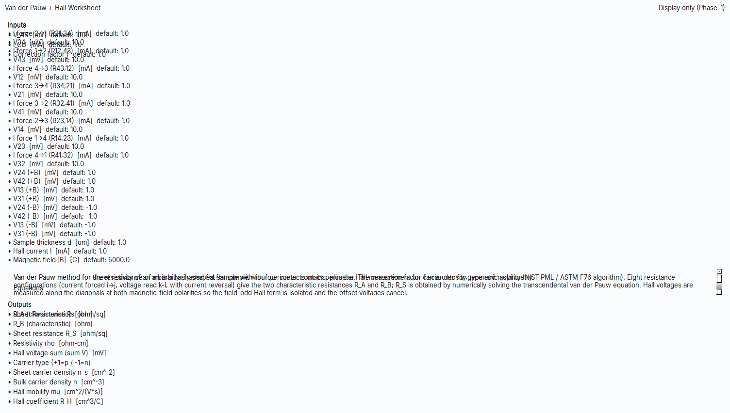
3.6 Van der Pauw + Hall Worksheet — calc:van_der_pauw_hall
By adding a magnet (magnetic field) to the sheet-resistance measurement, you also learn the type of the charge carriers in the material (are they electrons or holes?), their concentration, and how fast they move (mobility). Like a crosswind pushing a river's current toward the bank; the magnetic field pushes the charges sideways and from the small resulting voltage you count the carriers.
Physical background: When a B field perpendicular to a current-carrying sample is applied, the moving charges accumulate on one side by the Lorentz force, and a Hall voltage arises perpendicular to the current; the sign of this voltage gives the carrier type (n or p), and its magnitude gives the concentration (fewer carriers → larger Hall voltage). When the sheet resistance (without B) is combined with the Hall data (with B), the mobility µ = 1/(q·n_s·R_S) is obtained; reversing the current direction and the B polarity and averaging erases contact and thermoelectric offsets.
- Why it is done: to determine, in one go, a semiconductor's type (n/p), carrier concentration, and mobility.
- What it teaches / measures: sheet resistance R_S / resistivity ρ; carrier type = the sign of the Hall voltage (+1=p / −1=n); sheet carrier concentration n_s (cm⁻²) and bulk concentration n (cm⁻³) = the number of charges per unit area/volume; Hall mobility µ (cm²/Vs) = how fast the carriers drift per unit field; Hall coefficient R_H.
- Typical values and interpretation: rough orders of magnitude — µ ~ 10²–10³ cm²/Vs in crystalline Si, ~10³–10⁴ in high-mobility GaAs, <1–10 in amorphous/organic semiconductors; at low doping the concentration is small/mobility high, and at heavy doping the reverse. n_s or n should come out in an order of magnitude consistent with the measured doping.
- Common mistakes / cautions: entering B in tesla instead of gauss (or vice versa) (a 10⁴-fold error in concentration); misreading the type sign in a weak/noisy Hall voltage; skipping the offset subtraction by reversing the B polarity; entering the thickness incorrectly and corrupting the n_s↔n conversion.
- Where it is used: doping-level verification, research on new semiconductor materials.
A full NIST/ASTM F76 worksheet: 8 resistivity I/V configurations + 8 Hall voltages → sheet resistance, resistivity, carrier concentration/type, and Hall mobility. The inputs are gathered into four groups (Resistivity R_A, Resistivity R_B, Hall +B, Hall −B) plus Geometry & Field.
| Input group | Content | Unit |
|---|---|---|
| Resistivity R_A | i_21,v_34 · i_12,v_43 · i_43,v_12 · i_34,v_21 | mA / mV |
| Resistivity R_B | i_32,v_41 · i_23,v_14 · i_14,v_23 · i_41,v_32 | mA / mV |
| Hall (+B) | V24, V42, V13, V31 | mV |
| Hall (−B) | V24, V42, V13, V31 | mV |
| Geometry & Field | thickness d (µm), Hall current I (mA), |B| (G/gauss) | — |
Formulas and outputs
| Output | Formula | Unit |
|---|---|---|
| R_A (characteristic) | ((v34/i21)+(v43/i12)+(v12/i43)+(v21/i34))/4 | Ω |
| R_B (characteristic) | ((v41/i32)+(v14/i23)+(v23/i14)+(v32/i41))/4 | Ω |
| Sheet resistance R_S | vdp_rs(R_A, R_B) — numerical solution | Ω/sq |
| Resistivity ρ | R_S·d·1e-4 | Ω·cm |
| Hall voltage sum | (V24+V42+V13+V31)₊B − (…)₋B | mV |
| Carrier type | copysign(1, ΣV) (+1=p / −1=n) | — |
| Sheet carrier conc. n_s | 8e-8·I·B / (q·|ΣV|) | cm⁻² |
| Bulk carrier conc. n | n_s / (d·1e-4) | cm⁻³ |
| Hall mobility µ | 1 / (q·n_s·R_S) | cm²/(V·s) |
| Hall coefficient R_H | type·µ·ρ | cm³/C |
The sheet resistance is found by solving the transcendental van der Pauw equation numerically (NIST/ASTM F76, Eq. 3):
exp(−π·R_A/R_S) + exp(−π·R_B/R_S) = 1vdp_rs solves this by Newton iteration; the function is strictly monotonic in R_S and the root is unique. The symmetric guess π·(R_A+R_B)/(2·ln2) is an excellent start. q = 1.602176634e-19 C. The 8e-8 factor jointly includes the gauss→tesla and m⁻²→cm⁻² conversions and the factor of 8 arising from ΣV summing the four Hall voltages at each polarity (ΣV ≈ 8·V_H). Reversing B and subtracting isolates the Hall term and erases the offsets. The carrier type is encoded numerically: +1 = p-type (holes), −1 = n-type (electrons).
Standard: IEEE 1620 · ASTM F76 · NIST PML · GUM.
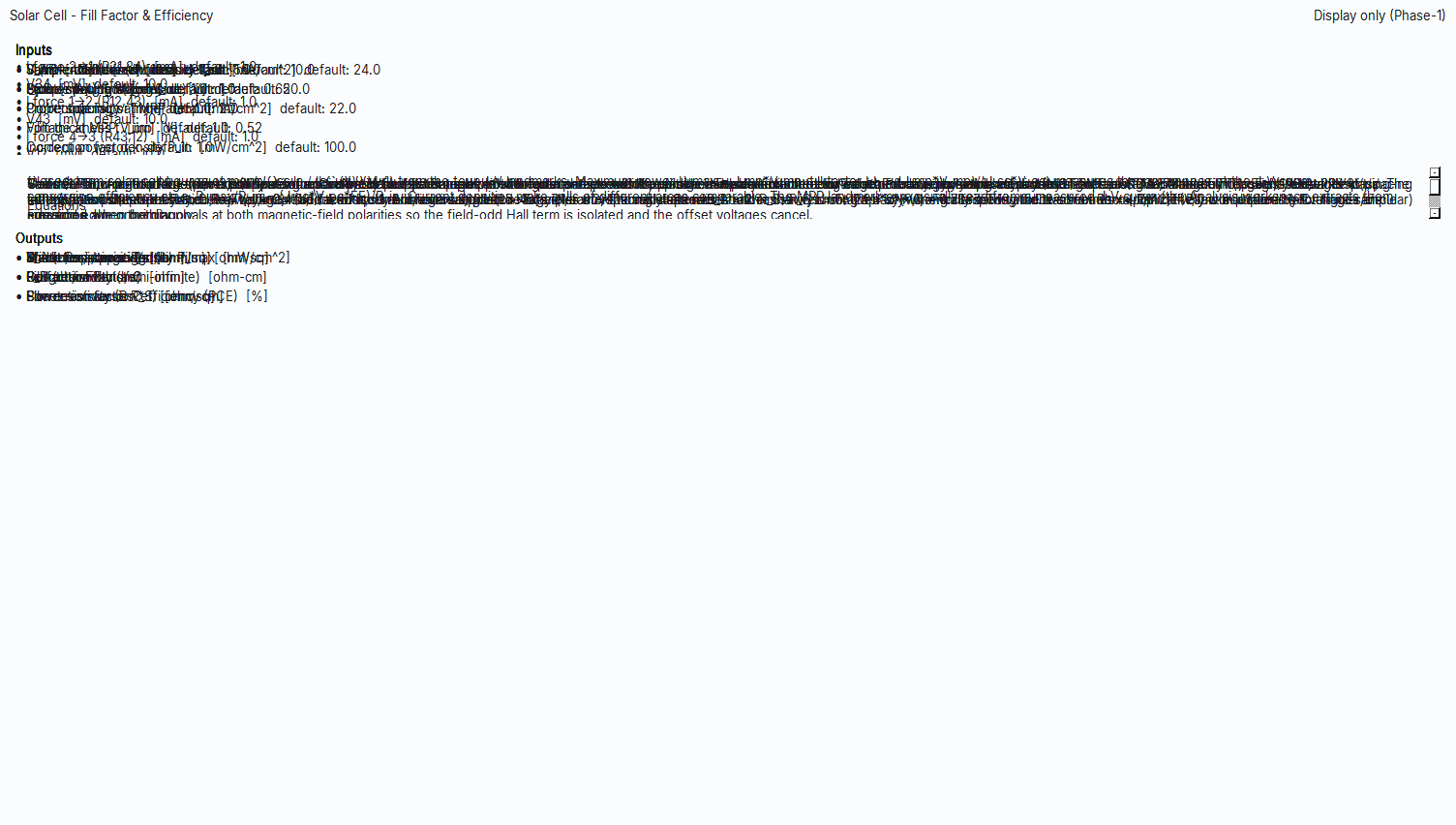
vdp_rs raises an error. Averaging the eight configurations (with current direction reversed) suppresses contact and thermoelectric offsets.3.7 Solar Cell — Fill Factor & Efficiency — calc:pv_metrics_manual
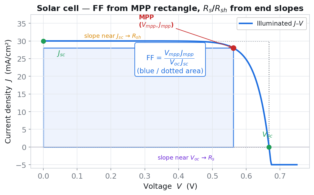
It summarizes how good a solar cell is with a few numbers: what percentage of the incident light it converts to electricity (efficiency, PCE) and how "full/ideal" the current-voltage curve is (fill factor, FF). FF measures how much the curve resembles a rectangle; the fuller the corner, the better the cell.
Physical background: The J-V curve of an illuminated cell gives the short-circuit current J_sc at V=0 and the open-circuit voltage V_oc at J=0; between the two it makes a "knee" and at one point produces maximum power (P_max = J_mp·V_mp). The sharper this knee, the higher the FF; series resistance (Rs) flattens the knee and pulls the current down, while a low shunt resistance (Rsh) pulls the voltage down, both degrading FF. For this reason FF is the ratio of the real power area of the curve to the ideal rectangle (J_sc·V_oc) area.
- Why it is done: to compare the performance of different solar cells fairly and under standard conditions.
- What it teaches / measures: P_max (mW/cm²) = the maximum power point; fill factor FF (0–1) = the rectangularity of the curve / the series-shunt resistance balance; power conversion efficiency PCE (%) = the ratio of the generated electrical power to the incident light power.
- Typical values and interpretation: FF > 0.7 is a good cell; FF < 0.5 is a sign of high Rs or low Rsh. Rough efficiency orders of magnitude: commercial crystalline Si ~18–24%, lab/perovskite cells over a wide range, immature technologies <10%.
- Common mistakes / cautions: not setting the illumination/spectrum to the standard (AM1.5G, 100 mW/cm², 25 °C); reading J_mp/V_mp from the wrong inflection point; FF > 1 or J_mp > J_sc indicates a sign/inflection-point error.
- Where it is used: photovoltaic research, production-line quality control, cell comparison tables.
It quickly computes solar-cell performance numbers manually from four J-V inflection points. Because current densities are used, cells of different areas can be compared directly.
| Parameter | Unit | Description | Default |
|---|---|---|---|
| Short-circuit current dens. J_sc | mA/cm² | Current density at V=0 | 24.0 |
| Open-circuit voltage V_oc | V | Voltage at J=0 | 0.65 |
| Current dens. at MPP J_mp | mA/cm² | Maximum power point current | 22.0 |
| Voltage at MPP V_mp | V | Maximum power point voltage | 0.52 |
| Incident power dens. P_in | mW/cm² | Illumination power density | 100.0 |
| Output | Formula | Unit |
|---|---|---|
| Maximum power dens. P_max | J_mp·V_mp | mW/cm² |
| Fill factor FF | (J_mp·V_mp)/(J_sc·V_oc) | — |
| Power conversion efficiency (PCE) | (J_mp·V_mp)/P_in·100 | % |
FF measures the "rectangularity" of the J-V curve (the series/shunt resistance balance). Standard test condition: AM1.5G, P_in = 100 mW/cm² (1000 W/m²), 25 °C. In a physical cell, 0 < FF < 1, J_mp ≤ J_sc, V_mp ≤ V_oc; FF > 1 points to an inflection-point/sign error.
Standard: IEC 60904-1 · GUM.
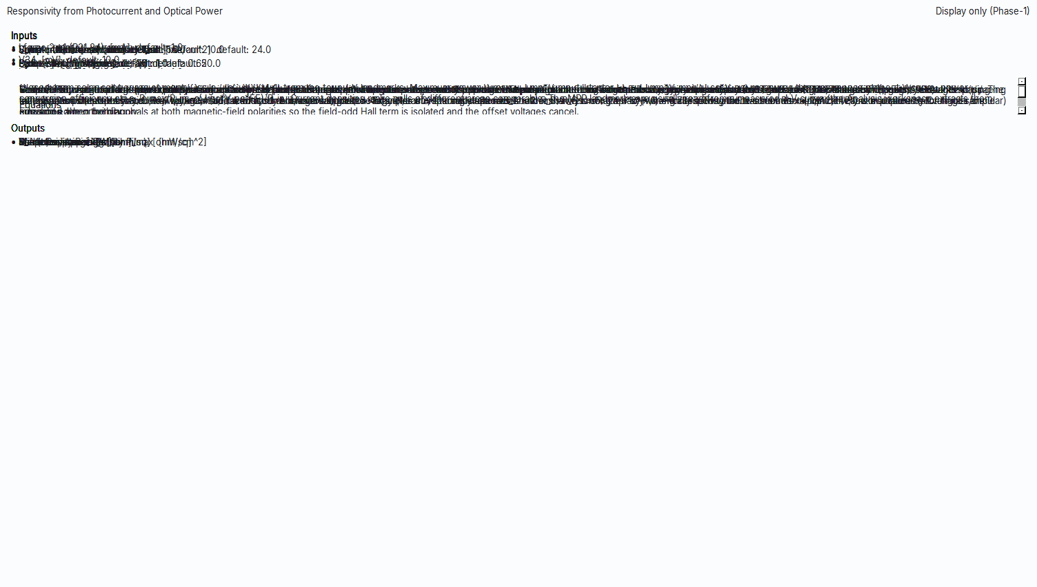
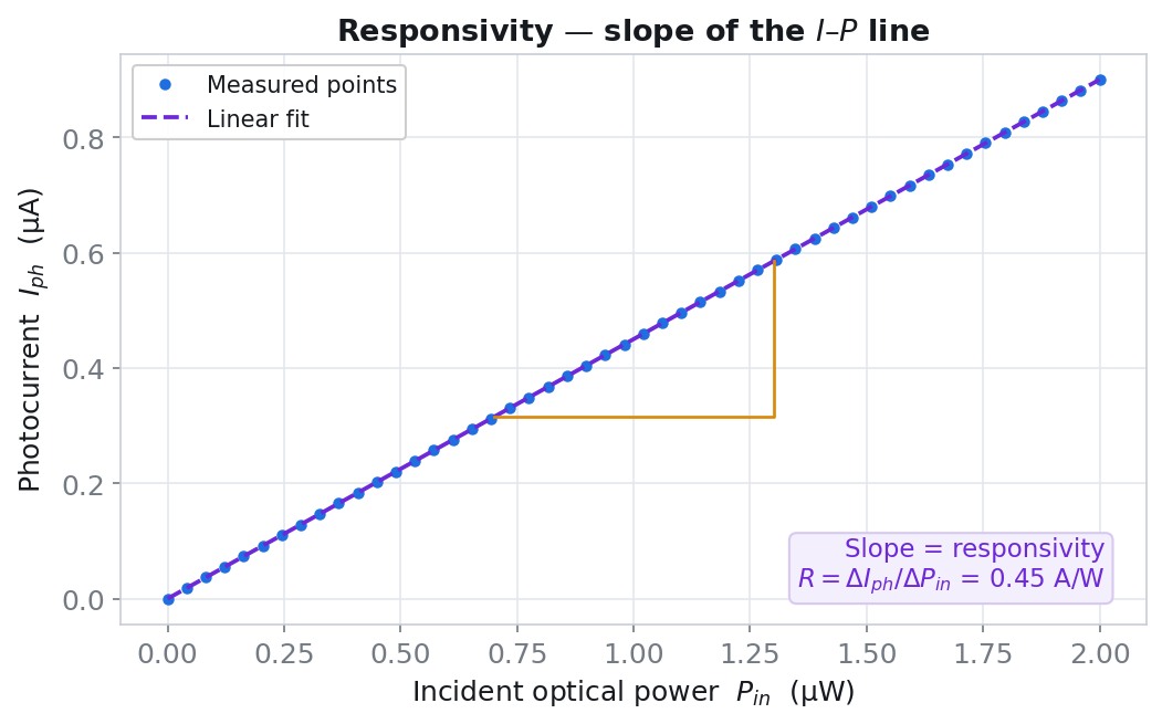
3.8 Responsivity (Photocurrent / Power) — calc:responsivity_from_power
It tells you how "responsive" a light detector is — that is, how many amperes of current it produces for each watt of light falling on it. Like how strongly a microphone converts sound into a signal; here, instead of sound there is light, and instead of a signal there is current.
Physical background: If the photons arriving at the detector have sufficient energy, they create electron-hole pairs, which turn into photocurrent; responsivity R = I_photo/P_det measures the efficiency of this conversion. R depends on wavelength: low-energy (long-wavelength) photons cannot cross the bandgap, while very high-energy photons give less current per photon — which is why every R value is meaningful only together with a λ. In a device without internal gain, R is related to the external quantum efficiency via R = EQE·λ/1239.84.
- Why it is done: to quantify the electrical response of a photodetector to light.
- What it teaches / measures: responsivity R = I_photo/P_det (A/W) = the net photocurrent generated per unit optical power at the detector; the value depends on wavelength.
- Typical values and interpretation: in photodiodes without internal gain, R is typically ~0.1–1 A/W (e.g. a visible/near-IR Si photodiode ~0.5 A/W); R > ~1 A/W often means internal gain (avalanche/phototransistor).
- Common mistakes / cautions: you must use the power reaching the detector, not the source power; forgetting to subtract the dark current; reporting the result without recording the wavelength at which it was taken.
- Where it is used: photodiode/sensor characterization, selection of optical-communication and imaging components.
Detector responsivity is the ratio of the net photocurrent to the incident optical power.
| Parameter | Unit | Description | Default |
|---|---|---|---|
| I_photo | A | Net photocurrent (dark current subtracted) | 1e-6 |
| P_det | W | Optical power incident on the detector aperture | 1e-6 |
| Output | Formula | Unit |
|---|---|---|
| Responsivity | R = I_photo / P_det | A/W |
Use the power at the detector, not the source power. Responsivity depends on wavelength; record the wavelength alongside the result. Source: Saleh & Teich, Fundamentals of Photonics.
4. GUM uncertainty propagation (optional, in every calculator)
No measurement is perfectly exact; every input has a small margin of error. This feature passes the "± how much" uncertainty in the inputs through the formula and carries it to the result as "± how much", and shows which input contributes most to the error. Like calculating how much the small deviations in the flour and sugar measurements in a recipe carry over into the cake.
- Why it is done: to report a result scientifically and honestly as "this value ± this much".
- What it teaches / measures: the combined uncertainty u_c, the expanded uncertainty U = k·u_c, and the percentage contribution budget of the inputs.
- Where it is used: accredited laboratory reports, calibration, standards-compliant statements of results.
In every calculator panel there is an Uncertainty (GUM) checkbox, off by default. When you turn it on, each numeric input gains a ± u standard-uncertainty field and a distribution selector; the outputs are shown as value ± U. Two complementary methods are used.
GUF — first-order linear propagation (JCGM 100:2008 / GUM): Sensitivity coefficients are computed via a numerical Jacobian (central finite difference, with a one-sided fallback at a domain boundary). The inputs are assumed uncorrelated:
u_c²(y) = Σᵢ (∂y/∂xᵢ)² · u(xᵢ)²Each output also carries an uncertainty budget: the percentage share of each input in the output variance (the NIST Uncertainty Machine "hero metric"). The panel shows these shares as a bar chart.
Monte Carlo — GUM-S1 (JCGM 101:2008): Each uncertain input is sampled from its distribution (normal / uniform / triangular — each scaled so that its standard deviation equals u); the spec is evaluated for each draw, by default 20,000 draws, and the mean, std (= u), and 95% coverage interval of the output are found from percentiles. It cross-validates the GUF for nonlinear models. It runs only on an explicit "Monte Carlo" click, on the GUI thread (sub-second).
| Control | Unit | Description | Default |
|---|---|---|---|
| ± u (per input) | input unit | Standard uncertainty (0 = exact) | 0.0 |
| Distribution | — | Normal / Uniform / Triangular (affects only Monte Carlo) | Normal |
| k (coverage factor) | — | U = k·u_c; k≈2 → ~95% | 2.0 |
Distribution half-widths: uniform a = u·√3, symmetric triangular a = u·√6 (both have a std of u). The expanded uncertainty is U = k·u_c; k only scales the display (u_c and the budget shares are independent of k), so a change in k is reflected instantly without re-propagation.
fpp_rect_corr / fpp_thick_corr), the GUF finite-difference sensitivity is biased due to the kink at the table node points; near these points prefer Monte Carlo (which samples the actual interpolation).5. Central Physics/Mathematics Reference
This section compiles, in one place, the derivation mathematics that the application uses across all of its workspaces (Measurement, Analysis, Calc). The equations are universal; in the application, per-quantity GUM uncertainty is still PLANNED (except for the Calc calculators — they use the GUM core in §4 live).
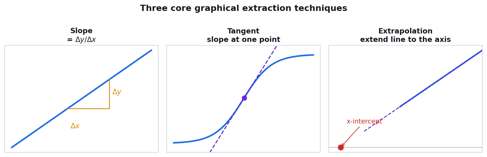
Nearly all of the physical quantities below are read from a graph with three basic operations: taking the slope of a line, drawing a tangent at a point, and extrapolating a line to an axis. First a transform that linearizes the data is chosen (e.g. log I_d, √I_d, ln I, 1/C², log–log), then these three operations are applied.
- Step: the slope = Δy/Δx is taken between two points in a linear region; if the data is curved, a tangent is drawn at the point of interest and its slope is read.
- Step: the line/tangent is carried to the data-free axis (usually the x-axis) by extrapolation and the axis intercept is read.
- Result: the slope and intercept are converted to the parameter by the relevant closed-form formula (e.g. mobility/ideality/doping from the slope; V_th/V_bi from the x-intercept; SS from the inverse of the slope).
5.1 Fundamental constants (CODATA 2019)
| Constant | Symbol | Value | Unit |
|---|---|---|---|
| Elementary charge | q | 1.602176634e-19 | C (exact) |
| Boltzmann constant | k_B | 1.380649e-23 | J/K (exact) |
| Planck constant | h | 6.62607015e-34 | J·s (exact) |
| Speed of light | c | 299792458.0 | m/s (exact) |
| Thermal voltage @300 K | V_T(300) | k_B·300/q ≈ 0.025852 | V |
| SS thermal limit @300 K | — | (k_B·300/q)·ln10·1e3 ≈ 59.53 | mV/dec |
| Photon energy product | h·c/q | 1239.84193 | eV·nm |
| van der Pauw geometric factor | π/ln2 | 4.5324 | — |
vdp_measurement.py measurement driver uses q = 1.602e-19 (3 significant figures); this means a ~0.01% systematic shift in carrier concentration. The van der Pauw + Hall worksheet in Calc, by contrast, uses the exact CODATA value (1.602176634e-19).5.2 Threshold voltage Vth — three methods
It is the threshold value at which a transistor "turns on" — that is, the gate voltage rises enough for the channel to begin conducting. Vth is the most fundamental number defining the on/off behavior of the transistor. Like the smallest opening point at which a faucet starts to flow; below that point there is almost no current.
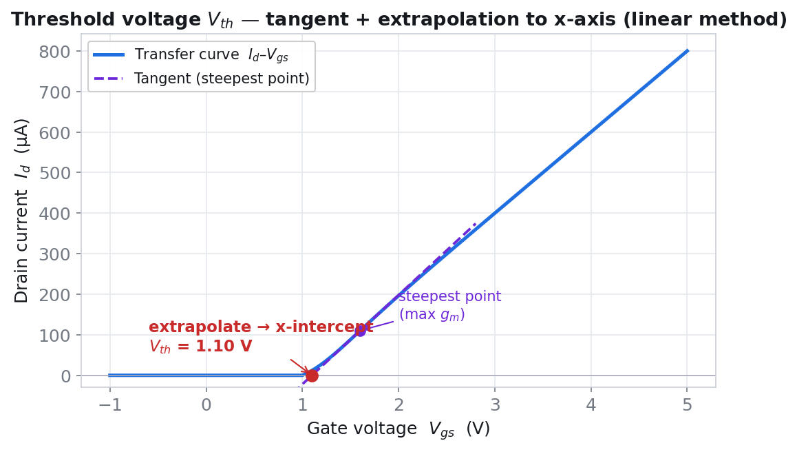
Physical background: Below Vth there are not enough carriers in the channel and only an exponential (diffusion-driven) sub-threshold current flows; when Vgs reaches the threshold, a conductive channel (inversion/accumulation layer) forms beneath the insulator. Above the threshold, since the channel charge increases as ≈ Cox·(Vgs−Vth), the current rises linearly with Vgs in the linear region and quadratically in saturation — which is why extrapolating the linear part of the Ids–Vgs (or √Ids–Vgs) curve back gives Vth. Because the "knee" is soft, there is no single exact value; therefore three separate methods are presented side by side for consistency.
- Why it is done: to know at what voltage the transistor switches on, and to compare device/process consistency.
- What it teaches / measures: Vth (V) = the threshold at which the channel turns on. Three methods: max-gm tangent = linear extrapolation from the steepest point (the most common); √Ids saturation = from the squareness of the saturation current (√Ids–Vgs linear); Y-function (Ghibaudo) = a series-resistance-free, mobility-independent estimate (comes with the fit quality y_r2).
- Typical values and interpretation: the sign/magnitude depend on the device (enhancement-mode n-FET has Vth > 0, p-FET < 0; the reverse for depletion mode). When the three methods come out close to one another (e.g. within ~0.1 V) it is a healthy measurement; a large discrepancy is a sign of series resistance, traps, or a poor line fit.
- Common mistakes / cautions: confusing the operating region (the linear method needs a small Vds, the saturation method a large Vds); overlooking that the max-gm method shifts Vth when series resistance is high; neglecting the forward/reverse difference in a hysteretic (bidirectional) sweep.
- Where it is used: TFT/FET design, circuit operating-point selection, production-stability monitoring.
| Method | Formula | Field / standard |
|---|---|---|
| Max-gm tangent (linear) | Vth = Vgs* − Ids*/gm_max | vth_v; IEC 60747-7 |
| √Ids saturation | √Ids ∝ (Vgs−Vth); Vth = Vgs* − √Ids*/m | vth_v / vth_sat_v |
| Y-function (Ghibaudo) | Y = Ids/√gm; Vth_y = −intercept/slope | vth_y_v; carries y_r2 |
Here gm = dIds/dVgs (central difference, one-sided at the ends), and gm_max is the largest |gm| in the forward sweep. The √Ids method comes from the relation Ids_sat = (W/2L)·µ·Cox·(Vgs−Vth)². If Vth is outside the physical window [Vgs_min − 2·span, Vgs_max + 2·span], it returns None.
The transfer curve measured at small V_ds (I_ds–V_gs, linear axis) is used; the point where the curve is steepest (where g_m is maximum) is chosen.
- Step: a tangent is drawn to the curve at the steepest point; the slope of the tangent is g_m,max.
- Step: the tangent is carried to the x-axis where the current goes to zero by extrapolation and the intercept is read.
- Result: the x-intercept is directly the threshold voltage —
V_th = V_gs* − I_ds*/g_m,max.
At large V_ds (saturation) a √I_ds–V_gs graph is plotted; since in saturation I_ds ∝ (V_gs−V_th)², this graph becomes a straight line.
- Step: a line is fitted to the linear region and its slope m is taken.
- Step: the line is carried to the x-axis by extrapolation; the intercept gives V_th —
V_th = V_gs* − √I_ds*/m. - Result: from the same slope, the saturation mobility
µ_sat = m²·2L/(W·C_ox)is found.
5.3 Mobility, subthreshold swing (SS), interface trap density (Dit)
These three numbers describe a transistor's "quality": mobility tells how fast the carriers flow, the subthreshold swing (SS) how sharply the transistor turns on and off, and Dit the density of defects (traps) at the insulator-semiconductor interface that disrupt the current. Mobility is "how clear the road is", SS is "how cleanly the light switch works", and Dit is "the number of potholes on the road".
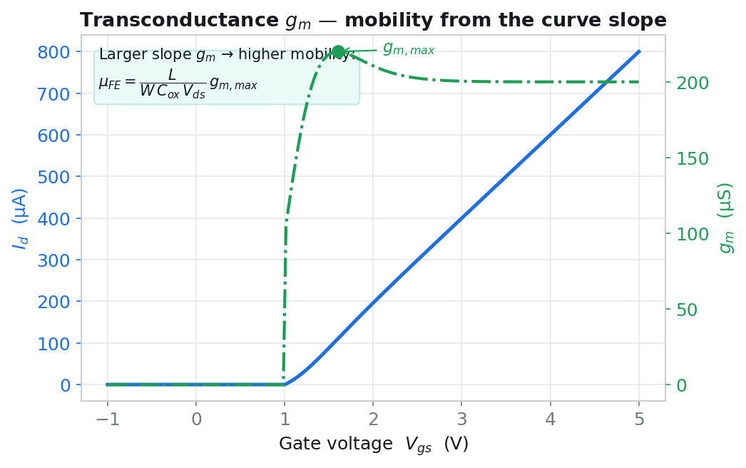
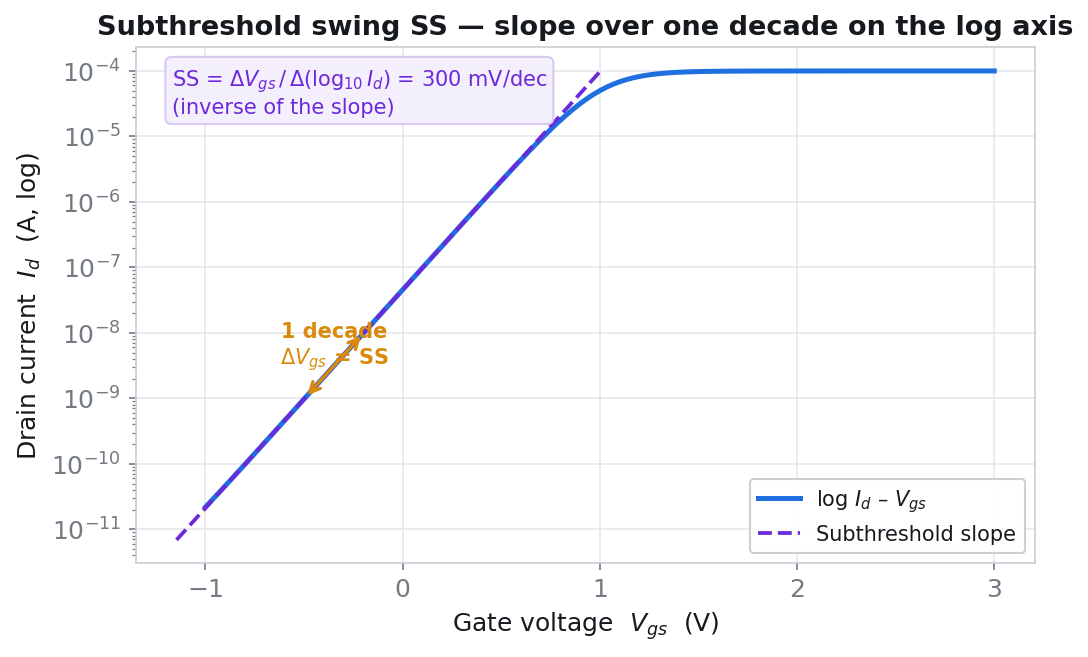
Physical background: Above the threshold, the current is proportional to the product of the channel charge and the mobility; therefore the larger gm (transconductance) is, the higher the mobility. Below the threshold the current is exponential in Vgs, so on a semi-logarithmic plot it becomes a straight line; the inverse of the slope of this line, SS, is the voltage required to increase the current tenfold. Traps at the interface "absorb" a portion of each additional voltage, flattening the slope; how much SS exceeds the ideal limit directly gives the trap density Dit.
- Why it is done: to evaluate the transistor's speed, switching sharpness, and material/interface quality.
- What it teaches / measures: mobility µ (cm²/Vs) = the ease with which carriers drift (from gm; field-effect, saturation, and Y-function versions); SS (mV/dec) = the gate voltage needed to change the current tenfold (switching sharpness); Dit (cm⁻²eV⁻¹) = interface trap density (from the excess of SS over the ideal limit).
- Typical values and interpretation: SS ~60–100 mV/dec is good (300 K theoretical lower bound ~59.53 mV/dec); SS > ~300 mV/dec means many traps/a poor interface. Rough mobility orders of magnitude: amorphous/organic <1–10, oxide (IGZO) ~10, poly-Si tens, crystalline Si hundreds cm²/Vs. A low Dit (≲10¹¹) is a sign of a clean interface, a high Dit of poor passivation.
- Common mistakes / cautions: reading SS on a linear axis (it must be measured on a log|Ids| axis, in the steepest decade window); mistaking an SS below the physical limit at 300 K as "good" (usually a measurement/fit error); entering Cox incorrectly and scaling mobility and Dit.
- Where it is used: new semiconductor/process development, device quality comparison, failure analysis.
| Quantity | Formula | Unit / field |
|---|---|---|
| Field-effect mobility µ_FE (linear) | µ_FE = gm_max / ((W/L)·Cox·|Vds|) | cm²/Vs; mu_fe_cm2_vs |
| Saturation mobility µ_sat | µ_sat = m²·2L/(W·Cox) | cm²/Vs; mu_sat_cm2_vs |
| Y-function mobility µ₀ | µ₀ = slope²/((W/L)·Cox·|Vds|) | cm²/Vs; mu0_y_cm2_vs |
| Subthreshold swing SS | SS = 1000/(d log10|Ids|/dVgs) (min window) | mV/dec; ss_mv_dec |
| Interface trap density Dit | Dit = (Cox/q)·(SS/SS_ideal − 1) | cm⁻²eV⁻¹; dit_cm2_ev |
| Ideal SS limit | SS_ideal = (k_B·T/q)·ln10, T=300 K | V/dec |
Mobility outside the physical window [1e-4, 1e4] cm²/Vs returns None. If SS < ~59.53 mV/dec (at 300 K), a warning is written (a sub-thermal swing is physically impossible without a ferroelectric gate); the value is nonetheless reported, not silently corrected. When SS < SS_ideal, since Dit would be negative, it returns None.
w_um/l_um) is used, the mobilities come out directly in cm²/Vs — there is no 1e4 factor.From the transfer curve in the linear region (I_ds–V_gs), the transconductance g_m = dI_ds/dV_gs is extracted as a derivative (slope).
- Step: the slope (g_m) at each point of the curve is computed; the largest value is taken as g_m,max.
- Step: no extrapolation is needed; the peak slope is used directly.
- Result:
µ_FE = g_m,max / ((W/L)·C_ox·|V_ds|).
The transfer curve is plotted semi-logarithmically (log₁₀|I_ds|–V_gs); since the current is exponential in the subthreshold region, it appears as a straight line on this axis.
- Step: in the steepest one-decade (10×-current) window, the tangent/slope Δ(log₁₀ I_ds)/ΔV_gs is taken.
- Step: no extrapolation is needed; SS is the inverse of this slope.
- Result:
SS = 1000/(d log₁₀|I_ds|/dV_gs)[mV/dec]; interface trapsD_it = (C_ox/q)·(SS/SS_ideal − 1).
5.4 Diode/Schottky · PV · photodetector core equations
This table gathers the key numbers defining light- and junction-based devices: how "ideal" a diode behaves (ideality n), the energy barrier at a metal-semiconductor contact (Schottky Φ_B), solar-cell performance (FF/PCE), and a detector's ability to convert light to electricity (EQE) together with its power to see the weakest signal amid noise (specific detectivity D*). Each is like a report-card item summarizing "how well the device does its job" with a single grade.
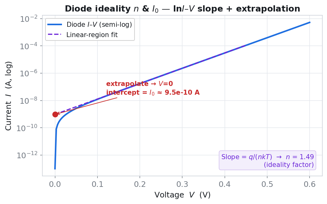
Physical background: In an ideal diode the current is exponential in voltage (I ∝ exp(qV/nkT)); therefore the ln(I)–V plot is linear, and from its slope the ideality n and from its intercept the saturation current I0 are read. At high voltage, series resistance bends this line (Cheung's method separates it). In a Schottky (metal-semiconductor) contact, the current is determined by carriers crossing the barrier via thermionic emission; the smaller I0 is, the higher the barrier Φ_B. In a photodetector, the incoming photons turn into carriers and the carriers into current; EQE quantifies this photon→electron efficiency, while D*/NEP quantify the smallest detectable signal relative to the noise floor.
- Why it is done: to quantify the performance of diodes, solar cells, and photodetectors with standard quantities.
- What it teaches / measures: ideality n = an indicator of the conduction mechanism (n≈1 ideal diffusion, n≈2 depletion-region recombination); I0 = leakage/saturation current; Schottky barrier Φ_B (eV) = the metal-semiconductor energy barrier; FF/PCE = solar-cell fill factor and efficiency; EQE/IQE = external/internal quantum efficiency (electrons collected per incident / absorbed photon); D* (Jones) and NEP (W) = the detector's noise-limited sensitivity (large D*, small NEP = good).
- Typical values and interpretation: in a good diode n ~1–1.5; n > 2 points to recombination/leakage/series-resistance problems. Φ_B is typically of order ~0.5–0.9 eV depending on the material pair. EQE in a good cell can exceed 80% at the peak wavelength; IQE ≥ EQE (since reflection is removed). The larger D* (e.g. ~10¹⁰–10¹³ Jones), the weaker the light the detector can see.
- Common mistakes / cautions: performing the ln(I)–V fit in the wrong region (leakage at low voltage and series resistance at high voltage distort the line); using the wrong Richardson constant A** or area A for Φ_B; confusing EQE with IQE; omitting the area/bandwidth (A·Δf) in the D* calculation.
- Where it is used: optoelectronic component development, solar-cell and sensor selection, performance comparison.
| Quantity | Formula | Standard |
|---|---|---|
| Ideality n | n = q/(k_B·T·slope) (ln I – V) | Schroder |
| Saturation current I0 | I0 = exp(intercept) | |
| Series resistance Rs (Cheung-1) | dV/d(ln I) = Rs·I + n·V_T | Cheung |
| Schottky barrier Φ_B | Φ_B = (k_B·T/q)·ln(A**·T²·A/I0) | thermionic emission |
| Richardson | ln(I0/T²) − 1/T slope; Φ_B = −slope·k_B/q | |
| FF (PV) | FF = Pmax/(Voc·Jsc) | IEC 60904-1 |
| PCE | PCE = 100·Pmax/Pin, Pin = irradiance/10 | IEC 60904-1 |
| Responsivity R | R = I_photo/P_det | IEC 60904-8 |
| External quantum efficiency EQE | EQE = R·1239.84/λ_nm | |
| Internal quantum efficiency IQE | IQE = EQE/(1 − R_refl) | |
| Linearity α / LDR | I = C·P^α; LDR = 20·log10(Pmax/Pmin) [dB] | IEC 60904-10 |
Since the diode current is exponential in voltage (I ∝ exp(qV/nkT)), the ln I–V plot is linear in the mid-voltage region.
- Step: the low-voltage (leakage) and high-voltage (series resistance) ends are excluded; a line is fitted to the middle region and its slope is taken.
- Step: the same line is carried to V=0 by extrapolation; the y-intercept is ln I₀.
- Result:
n = q/(k_B·T·slope)andI₀ = exp(intercept).
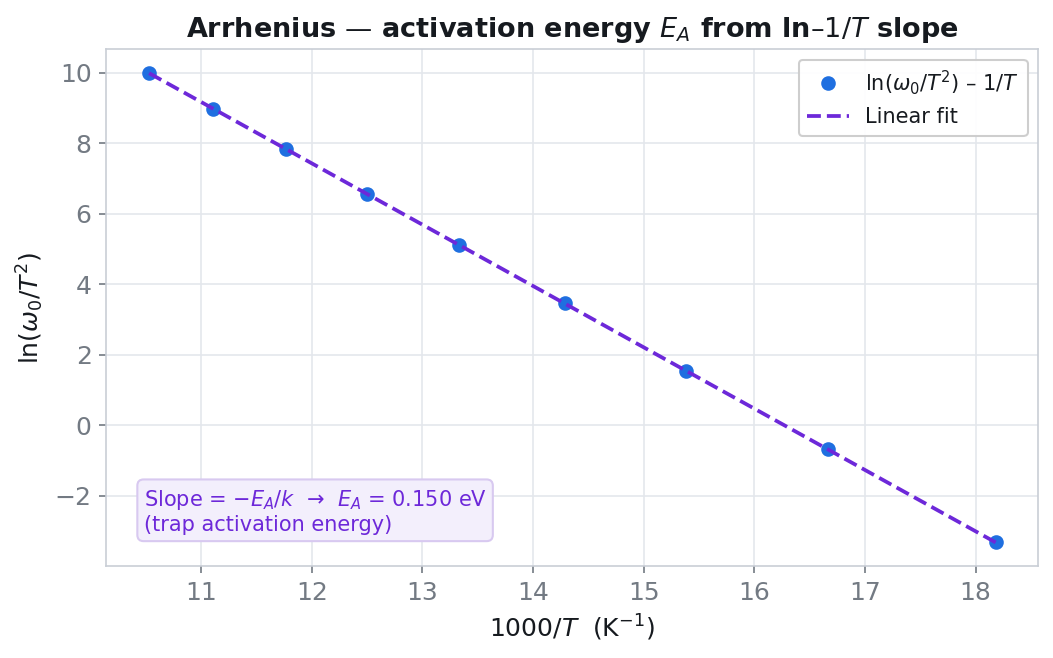
In a thermally activated process (e.g. Richardson: the variation of saturation current with temperature), the ln(I₀/T²)–1/T plot is linear; its slope carries the energy barrier.
- Step: a line is fitted to the points at different temperatures and its slope is taken.
- Step: the slope is converted to energy by the Arrhenius relation (no extrapolation needed).
- Result: the barrier
Φ_B = −slope·k_B/q(more generally, the activation energy E_A = −slope·k_B).
The illuminated J-V curve is used; the maximum power point (MPP), where the product J·V is largest, is found on the curve.
- Step: a rectangle (J_mp × V_mp) inscribed in the curve is placed at the MPP; J_sc and V_oc are read from the axis intercepts.
- Step: the slopes at the ends reveal the series/shunt resistance (R_s near V_oc, R_sh near J_sc).
- Result:
FF = (J_mp·V_mp)/(J_sc·V_oc)andPCE = (J_mp·V_mp)/P_in·100.
Noise and detectivity (noise.py):
i_density = i_noise / √Δf                  [A/√Hz]
NEP       = i_noise / R                     [W]            (noise-equivalent power)
D*        = R·√(A·Δf) / i_noise             [Jones]        (specific detectivity)
i_shot    = √(2·q·|I_dark|·Δf)              [A]            (shot noise)
i_thermal = √(4·k_B·T·Δf / Rsh)            [A]            (thermal/Johnson noise)
S(f) ∝ 1/f^γ  → γ = −slope(log S – log f);  corner frequency = white-floor intercept
Temporal response (temporal.py): rise/fall time from the 10–90 % / 90–10 % levels; BW_3dB ≈ 0.35/t_rise (Gaussian/RC); photo/dark ratio, SNR = 20·log10(|I_photo|/σ).
At a fixed wavelength, the net photocurrent is measured at different optical powers and the I_photo–P_in graph is plotted; in a linear detector this is a straight line.
- Step: a line is fitted to the data points and its slope is taken.
- Step: the line should pass through the origin; a nonzero intercept is a sign of dark current/stray light.
- Result: the slope is directly the responsivity —
R = I_photo/P_det[A/W] (record the wavelength alongside the result).
5.5 Resistance physics (collinear 4PP and van der Pauw)
This part connects the different faces of the question "how well does a material conduct electricity?": sheet resistance Rs is the practical measure for thin films, resistivity ρ is the thickness-independent intrinsic property of the material, and conductivity σ is the inverse of ρ. Like expressing the same property in different units; which one you use depends on whether the sample is a thin film or a bulk piece.
Physical background: The fact that a thin film has the same thickness everywhere makes it possible to fold the thickness into the resistance and express it as a single surface quantity, the sheet resistance Rs = ρ/t (unit: "ohms per square", because the resistance of a square area is independent of size). Resistivity ρ is material-specific and contains no geometry; when a Hall measurement is added, the same framework also yields the carrier concentration and mobility from the lateral voltage produced in a magnetic field.
- Why it is done: to convert a measured resistance into a material-specific, comparable quantity.
- What it teaches / measures: sheet resistance Rs (Ω/sq) = the practical resistance for a thin film with thickness folded in; resistivity ρ (Ω·cm) = the geometry-independent intrinsic conduction property (ρ = Rs·t); conductivity σ = 1/ρ (S/cm); with Hall, additionally R_H, n, µ.
- Typical values and interpretation: rough orders of magnitude for ρ — good metals ~10⁻⁶ Ω·cm, semiconductors ~10⁻³–10² Ω·cm depending on doping, insulators >>10⁶ Ω·cm; σ is the inverse. The interpretation of sheet resistance is the same as the film orders of magnitude in §3.1 and §3.5.
- Common mistakes / cautions: confusing the thin-film (Rs = ρ/t) and bulk formulas; entering the thickness in the wrong unit (µm↔cm) and shifting ρ; applying the carrier-concentration conversion
n_s = n·tincorrectly in Hall (see the historical-error warning alongside). - Where it is used: film and bulk sample comparison, material selection, process verification.
Rs = (π/ln2)·|R| ≈ 4.5324·R [Ω/sq]
ρ = Rs·t (thin film) ; ρ = 2π·s·|R| (bulk) [Ω·cm]
σ = 1/ρ [S/cm]
van der Pauw: exp(−π·R_A/Rs) + exp(−π·R_B/Rs) = 1 (numerical root)
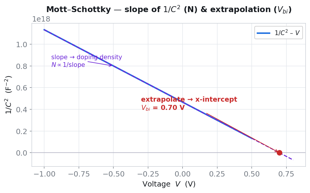
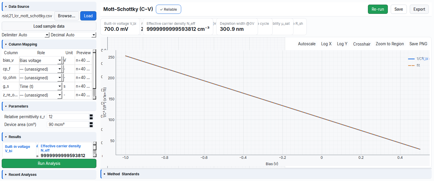
Hall: R_H = VH·t/(I·B) ; n = 1/(|R_H|·q) ; µ = |R_H|/ρvdp_measurement.py computes the sheet carrier concentration as n_s = n_bulk·t·1e7; since the correct relation is n_s = n_bulk·t (cm⁻³·cm = cm⁻²), this is 10⁵ times too large (AUDIT HIGH-004). The van der Pauw + Hall worksheet in Calc uses the correct relation n_s = 8e-8·I·B/(q·|ΣV|); keep this difference in mind when comparing.5.6 Mott-Schottky (C-V depth profile) and RUS/RPS
Two different "depth probes": Mott-Schottky extracts a junction's doping concentration and built-in voltage from the variation of capacitance with voltage; RUS/RPS, on the other hand, tracks how a sample's stiffness (elastic modulus) changes with temperature, from its vibration (resonance) frequency. Mott-Schottky maps the doping with an electrical "sonar"; RUS taps the sample like a bell and infers the material's stiffness from the tone of the sound.
Physical background: In a reverse-biased junction, as the voltage increases the depletion region widens and the junction behaves like a capacitor whose plates move apart — the capacitance drops. Theory predicts that 1/C² is linear in voltage; the slope of this line gives the doping concentration, and its x-intercept gives the built-in voltage V_bi. In RUS, since the square of the resonance frequency is proportional to the stiffness/density ratio, the variation of f0² with temperature tracks the elastic modulus and appears as a softening at a phase transition.
- Why it is done: to determine a junction's doping profile (Mott-Schottky) or a material's phase-transition/stiffness behavior (RUS).
- What it teaches / measures: effective doping N_eff (cm⁻³) = the doping concentration from the slope of the 1/C²–V line; built-in voltage V_bi = the x-intercept (the junction's internal potential); depletion width W_d; in RUS the relative elastic modulus and softening at a phase transition.
- Typical values and interpretation: rough orders of magnitude for semiconductor doping ~10¹⁴–10¹⁹ cm⁻³ (low=light, high=heavy doping); the linearity of the 1/C²–V plot indicates uniform doping, while curvature indicates a depth-varying profile or a trap effect. V_bi is typically of order the bandgap (~half to one volt).
- Common mistakes / cautions: entering the wrong junction area A or dielectric constant ε_r and scaling N_eff; reading the slope from a non-linear part of the curve; neglecting that the measurement frequency/series resistance distorts C; trying to apply Mott-Schottky in forward bias (where the depletion narrows).
- Where it is used: semiconductor junction characterization, phase-transition/material-physics research.
Mott-Schottky (lcr_mott_schottky): effective doping, built-in voltage, and depletion width from a linear fit of 1/C² – V.
m = d(1/C²)/dV   →   N_eff = −2/(q·ε_r·ε0·A²·m)   [cm⁻³]
V_bi = −b/m  (x-intercept)
W_d(V) = ε_r·ε0·A / C
The uncertainty comes from the fit covariance: u(N)/N = u(m)/|m|. Standard: Sze, Physics of Semiconductor Devices (depletion capacitance + Mott-Schottky).
The capacitance measured in reverse bias is plotted as 1/C²–V; for uniform doping this plot is linear.
- Step: a line is fitted to the linear region and its slope m is taken.
- Step: the line is carried to the x-axis by extrapolation; the intercept gives the built-in voltage —
V_bi = −b/m. - Result: the effective doping from the slope
N_eff = −2/(q·ε_r·ε₀·A²·m).
RUS / RPS (resonant ultrasound spectroscopy) (rps_elastic_modulus): the square of the resonance frequency is proportional to the effective elastic stiffness over the density:
f0²(T) ∝ c_eff(T)/ρ → modulus_rel(T) = f0(T)² / f0(T_ref)²At a phase transition, modulus softening near Tc appears as modulus_rel → 0. GUM: u²(modulus_rel) = (2·f0/f0_ref²)²·u²(f0) + (−2·f0²/f0_ref³)²·u²(f0_ref) (independent fits). Standard: Migliori & Sarrao (1997) · ASTM E1876.
5.7 GUM uncertainty — Type-A, Type-B, and the coverage factor k
It splits where the uncertainty comes from into two: Type-A, by repeating the measurement many times and looking at the scatter (statistics); Type-B, from ready information such as a certificate, tolerance, or resolution. Then, with the coverage factor k, you widen the "± U" interval to the desired confidence level (e.g. 95%). Type-A is "weighing the same thing many times and looking at the spread", Type-B is "trusting the error margin on the scale's label".
- Why it is done: to classify the sources of uncertainty correctly and declare a reliable error margin.
- What it teaches / measures: Type-A/Type-B standard uncertainties, the combined u_c, and the expanded uncertainty U = k·u_c (k=2 → ~95%).
- Where it is used: calibration certificates, standards-compliant measurement reports, laboratory accreditation.
Measurement uncertainty is evaluated in two ways (ISO/IEC Guide 98-3:2008 = JCGM 100:2008):
| Type | Definition | Example |
|---|---|---|
| Type-A | Statistical analysis of repeated observations (sample standard deviation) | The standard error of the mean of N repeats s/√N |
| Type-B | From non-statistical information (calibration certificate, manufacturer tolerance, resolution) | Uniform-distribution half-width a → u = a/√3 |
- The combined standard uncertainty u_c is the combination of the individual u's by the sum-of-squares rule in §4.
- The expanded uncertainty
U = k·u_c; the coverage factor k gives the desired confidence level: for a normal output, k = 2 → ~95%, k = 3 → ~99.7%. k is adjustable in the panel (1.0–6.0). - The Calc panel presents each output as
value ± Uand shows each input's percentage share in the budget; Monte Carlo, on the other hand, gives the 95% coverage interval directly without assuming a distribution.
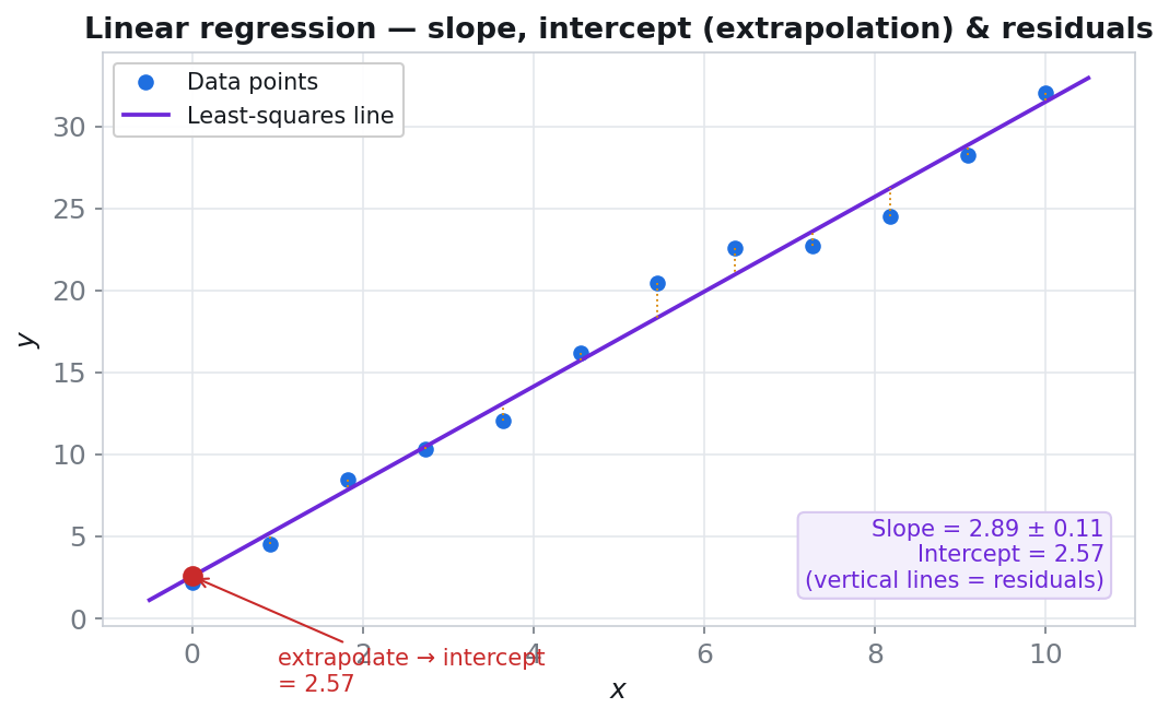
All of the slope/intercept extractions above are performed numerically by least-squares line fitting; this is the objective counterpart of "drawing a tangent by eye", and it also produces the uncertainty.
- Step: a line minimizing the squares of the vertical deviations is fitted to the linearized data (slope and intercept together).
- Step: the intercept is obtained by extrapolation to the required axis (the regression already gives the line's axis value).
- Result: the slope/intercept uncertainty comes from the residuals and the fit covariance; e.g. in Mott-Schottky
u(N)/N = u(m)/|m|.
6. Visual reference (calc_<key>.png)
A screenshot of each calculator module is given under the relevant subheading with the naming calc_<id>.png: calc_four_point_probe.png, calc_fpp_correction_circular.png, calc_fpp_correction_rectangular.png, calc_fpp_correction_thick.png, calc_sheet_resistance_vdp.png, calc_van_der_pauw_hall.png, calc_pv_metrics_manual.png, calc_responsivity_from_power.png. The workspace overview is shown with page_calc.png, the free-form formula notebook with ui_calc_formula_editor.png, and the GUM budget panel with ui_calc_uncertainty_budget.png. The theme-aware schematic drawing and legend in each module draw that measurement's geometry (contact/probe layout, the I source, the V meter, the B field, the J-V curve) on the fly with QPainter; no separate binary image file is carried.